Display device and array substrate as well as thin film transistor and manufacturing method thereof
A technology of thin film transistors and manufacturing methods, which is applied in the field of display devices, can solve problems such as damaging device stability and affecting product yield, and achieve the effects of improving yield, shortening process time, and avoiding impact
- Summary
- Abstract
- Description
- Claims
- Application Information
AI Technical Summary
Problems solved by technology
Method used
Image

Examples
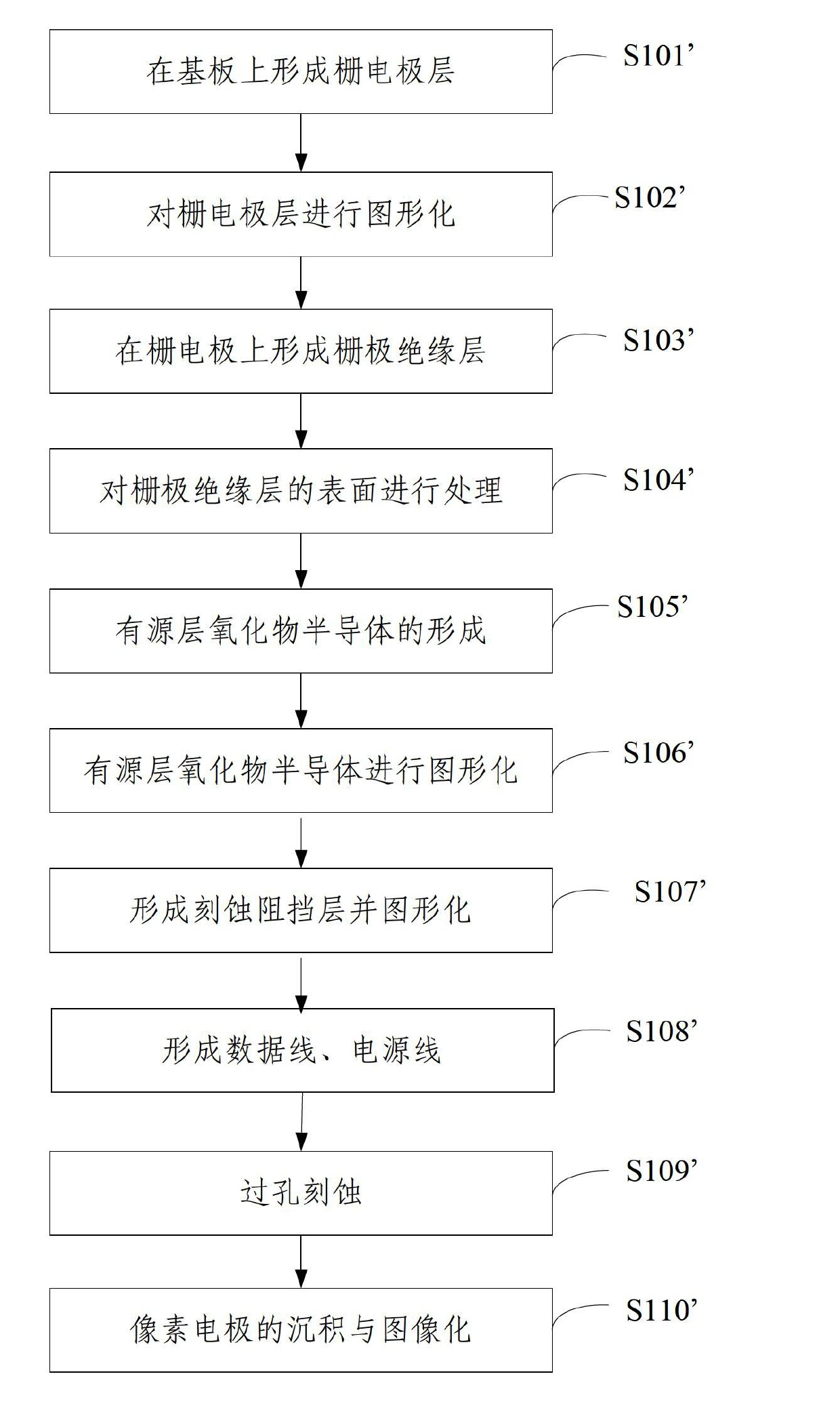
Embodiment 1
[0134] Such as image 3 As shown, as an embodiment of the present invention, the thin film transistor provided in the embodiment of the present invention is a thin film transistor structure in which the gate layer is located at the bottom layer. Specifically, the thin film transistor includes: a gate 302a on the substrate 301, a gate insulating layer and an active layer 306a respectively on the gate 302a. Wherein, the active layer 306a is an oxide semiconductor, the gate 302a is copper or a copper alloy, and the gate insulating layer is a single-layer structure, including a first gate insulating layer 303, and the first gate insulating layer 303 is silicon dioxide film, silicon nitride film, silicon oxynitride film, aluminum oxide film or titanium oxide film. The thickness of the first gate insulating layer 303 is 50nm˜500nm.
[0135] In the embodiment of the present invention, besides silicon dioxide film, silicon nitride film, silicon oxynitride film, aluminum oxide film o...
Embodiment 2
[0157] The difference between this embodiment and the first embodiment is that the thin film transistor provided by the embodiment of the present invention is a thin film transistor with a gate layer located on the top layer. Specifically, the thin film transistor includes: an active layer located on the substrate, a gate insulating layer located above the active layer, and a gate located above the gate insulating layer. Specifically, the structure and manufacturing method of the gate insulating layer are the same as those of the gate insulating layer in Embodiment 1, and will not be repeated here.
Embodiment 3
[0159] Such as Figure 5 As shown, the thin film transistor provided by the embodiment of the present invention is a thin film transistor structure in which the gate layer is located at the bottom layer. Specifically, the thin film transistor includes: a gate 312a on the substrate 311, a gate insulating layer and an active layer 316a respectively located above the gate 312a. Wherein, the active layer is an oxide semiconductor, the gate 312a is copper or a copper alloy, and the gate insulating layer is two layers, including a first gate insulating layer 313 and a second gate insulating layer 314, the first gate insulating layer 313 and the second gate insulating layer 314. The 313 layer is close to the gate 312a and is located above the gate. The second gate insulating layer 301 is close to the active layer 316a, wherein the first gate insulating layer 313 is a silicon nitride film or a silicon nitride oxide film, and the second gate insulating layer 301 is close to the active ...
PUM
| Property | Measurement | Unit |
|---|---|---|
| Thickness | aaaaa | aaaaa |
| Thickness | aaaaa | aaaaa |
| Thickness | aaaaa | aaaaa |
Abstract
Description
Claims
Application Information
 - Generate Ideas
- Intellectual Property
- Life Sciences
- Materials
- Tech Scout
- Unparalleled Data Quality
- Higher Quality Content
- 60% Fewer Hallucinations
Browse by: Latest US Patents, China's latest patents, Technical Efficacy Thesaurus, Application Domain, Technology Topic, Popular Technical Reports.
© 2025 PatSnap. All rights reserved.Legal|Privacy policy|Modern Slavery Act Transparency Statement|Sitemap|About US| Contact US: help@patsnap.com