Manufacturing method of infrared detector based on temporary release protective layer

A technology for infrared detectors and manufacturing methods, which is applied in semiconductor devices, final product manufacturing, sustainable manufacturing/processing, etc., and can solve problems such as adiabatic and thermal time constant disadvantages, structure and process complexity, etc.

Active Publication Date: 2012-09-19
ZHEJIANG DALI TECH
View PDF3 Cites 22 Cited by
  • Summary
  • Abstract
  • Description
  • Claims
  • Application Information

AI Technical Summary

Problems solved by technology

This will undoubtedly bring about the complexity of the structure and process, and have adverse effects on adiabatic and thermal time constants, etc.

Method used


Image

  • Manufacturing method of infrared detector based on temporary release protective layer
  • Manufacturing method of infrared detector based on temporary release protective layer
  • Manufacturing method of infrared detector based on temporary release protective layer

Examples


Embodiment Construction

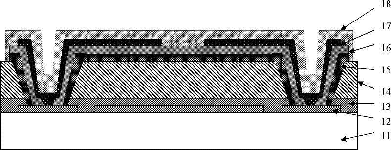
[0052] The preferred embodiments of the infrared detector manufacturing method provided by the present invention will be described in detail below in conjunction with the accompanying drawings, in order to further illustrate the technical methods and effects of the present invention.

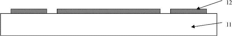
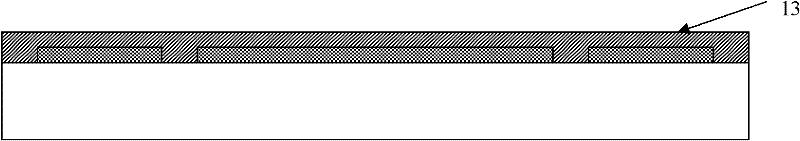
[0053] figure 1 It is a sectional view of the infrared detector of the present invention. The infrared detector includes: a semiconductor substrate 11, a metal layer 12, a dielectric layer 13, a sacrificial layer 14, a first temporary release protection layer 15, a sensitive layer 16, a metal electrode layer 17, The second layer temporarily releases the protective layer 18 .

[0054] Figure 2 is figure 1 The flowchart of the processing method of the infrared detector is shown. The infrared detector processing method of the present invention will be described in detail below in conjunction with FIG. 2 , and the present invention will be further described.

[0055] 2(a), fabricating and patter...


PUM


Abstract

The invention discloses a surface micromachining method for a microelectromechanical system based on a temporary release protective layer and particularly relates to a manufacturing method of an uncooled infrared detector. The manufacturing method comprises the following steps of: sequentially depositing a metal layer, an amorphous silicon sacrificial layer, a first temporary release protective layer of polyimide on a CMOS (complentary metal-oxide-semiconductor transistor) silicon substrate; manufacturing a sensitive layer and a metal electrode layer in a cascading way, and imaging the sensitive layer, the electrode layer and a microbridge structure; and finally manufacturing a second temporary release protective layer. When the sacrificial layer is released, firstly XeF2 is adopted for releasing the amorphous silicon sacrificial layer, and then O2 plasma is utilized for removing the temporary release protective layers after the release is completed. According to the manufacturing method of the infrared detector provided by the invention, compared with the prior art, the adopted temporary release protective layers are completely removed in the later period of manufacturing, thus not causing any influence on the microbridge performance, and being beneficial to the reduction of process difficulty and improvement of the performance of the detector.

Description

[0001] technical field [0002] The invention relates to the field of micro-electromechanical systems, in particular to a processing method for an uncooled infrared detector using a temporary release protective layer. Background technique [0003] At present, the uncooled infrared detector mainly adopts the microbolometer (Microbolometer) technology with a microbridge structure. It is characterized in that it adopts surface micromachining technology to manufacture a bridge-like microstructure suspended above the CMOS substrate and supported by slender cantilever beams, which is commonly referred to as a microbridge structure in the industry. The micro-bridge structure generally has at least two anchor holes, which are used as supporting points and the electrical connection between the pixel and the CMOS. It has at least one layer of sensitive layer material, currently widely used include vanadium oxide and doped amorphous silicon thin film. There is at least one layer of e...

Claims


Application Information

Patent Timeline
Patent Type & Authority Applications(China)
IPC IPC(8): H01L31/18
CPCY02P70/50
Inventor 姜利军池积光钱良山王景道黄河
Owner ZHEJIANG DALI TECH
Why Eureka
Try Eureka