Flip-chip type semiconductor luminescent device structure and manufacture method thereof

A technology for light-emitting devices and semiconductors, applied in semiconductor devices, electrical components, circuits, etc., can solve the problems of light quality degradation, light output reduction, and high refractive index, and achieve the effect of optimizing thickness, reducing absorption, and increasing light transmission.

Active Publication Date: 2012-09-19
XIAMEN SANAN OPTOELECTRONICS TECH CO LTD
View PDF4 Cites 12 Cited by
  • Summary
  • Abstract
  • Description
  • Claims
  • Application Information

AI Technical Summary

Problems solved by technology

[0004] However, different interfaces of the semiconductor layer have different degrees of reflection and absorption of light.
For example: the GaN crystal has a high refractive index, and the light emitted by it inside the crystal of the LED element does not completely pass through but is reflected inside, and is finally absorbed by the material to generate heat; moreover, usually light-emitting diode chips need to use organic materials Encapsulation, accompanied by the heat of this encapsulation material, will cause the quality of light to deteriorate, resulting in the problem of reduced light output

Method used


Image

  • Flip-chip type semiconductor luminescent device structure and manufacture method thereof
  • Flip-chip type semiconductor luminescent device structure and manufacture method thereof
  • Flip-chip type semiconductor luminescent device structure and manufacture method thereof

Examples


Embodiment Construction

[0033] The implementation of the present invention will be described in detail below in conjunction with the accompanying drawings and examples, so as to fully understand and implement the process of how to apply technical means to solve technical problems and achieve technical effects in the present invention. It should be noted that, as long as there is no conflict, each embodiment and each feature in each embodiment of the present invention can be combined with each other, and the formed technical solutions are all within the protection scope of the present invention.

[0034] The flip-chip semiconductor light-emitting device and its manufacturing method proposed by the present invention are mainly applied to gallium nitride-based semiconductor light-emitting devices, and are especially suitable for ultraviolet light-emitting diode devices with a wavelength between 100nm and 400nm.

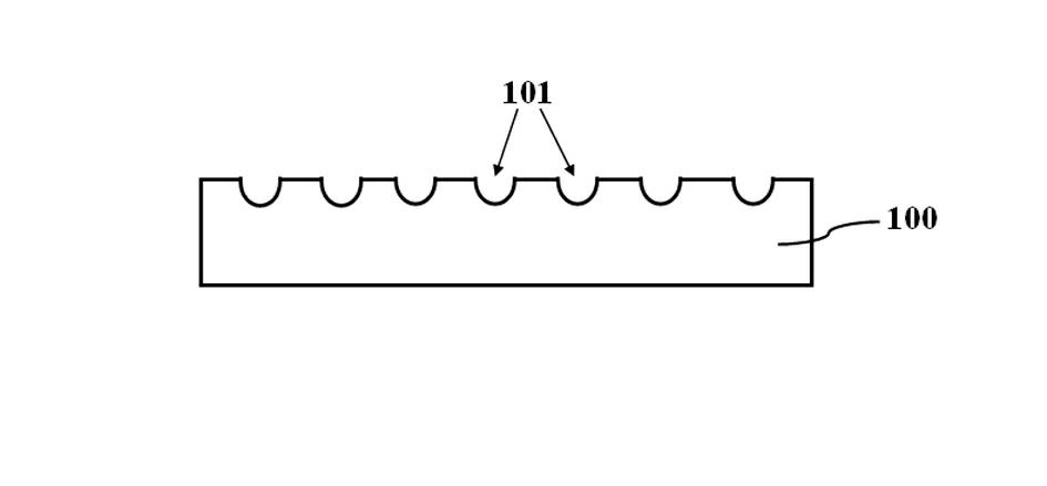
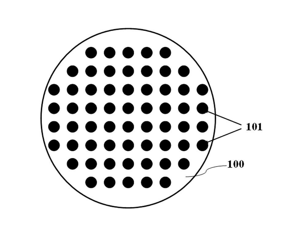
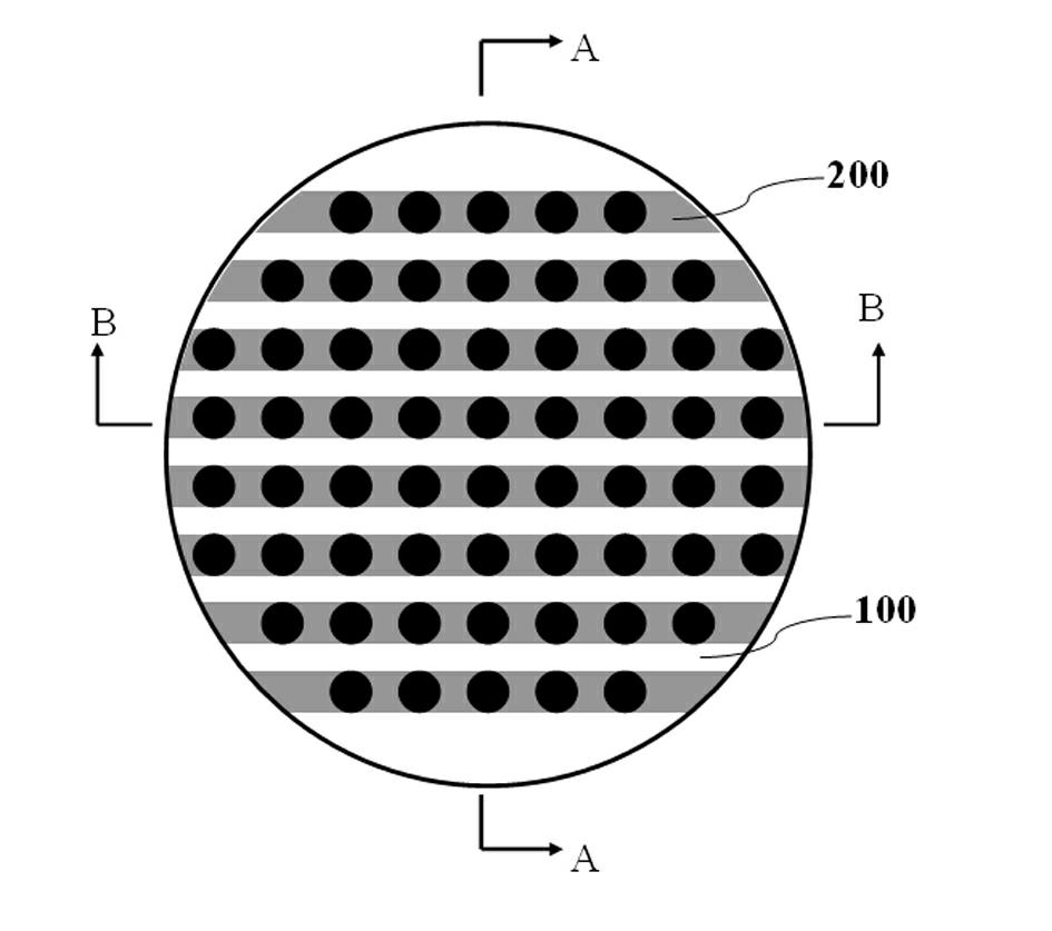
[0035] Such as figure 1 As shown, a flip-chip semiconductor light-emitting device includes:...


PUM


Abstract

The invention discloses a flip-chip type semiconductor luminescent device structure and a manufacture method thereof. The flip-chip type semiconductor luminescent device structure comprises a supporting base plate, a luminous epitaxial layer and a light-transmitting growth substrate, wherein the luminous epitaxial layer is located on the supporting base plate and is sequentially formed by a p-shaped semiconductor layer, a luminous active layer, an n-shaped semiconductor layer and a buffering layer, and the light-transmitting growth substrate is located on the luminous epitaxial layer. The flip-chip type semiconductor luminescent device structure is characterized in that a regular graphical air interlayer is located between the light-transmitting growth substrate and the luminous epitaxial layer and has optical matching thickness. By means of the graphical air interlayer located between the light-transmitting growth substrate and the luminous epitaxial layer and having the optical matching thickness, the effects of light transmitting and radiation can be achieved.

Description

technical field [0001] The invention belongs to the field of manufacturing semiconductor light emitting devices, and in particular relates to a flip-chip semiconductor light emitting device structure and a manufacturing method thereof. Background technique [0002] In recent years, in order to improve the luminous power and efficiency of III-nitride-based compound semiconductor light-emitting devices, thin-film device technology based on substrate transfer has been developed, such as depositing III-nitride thin films on sapphire substrates by MOCVD, and then transferring III-nitride The nitride film is bonded to the semiconductor or metal substrate by wafer bonding technology or electroplating technology, and then the sapphire substrate is removed by laser lift-off method; or the group III nitride film is deposited on the SiC or Si substrate, and then the group III The nitride film is bonded to the semiconductor or metal substrate by wafer bonding technology or electroplatin...

Claims


Application Information

Patent Timeline
Patent Type & Authority Applications(China)
IPC IPC(8): H01L33/20H01L33/00
Inventor 钟志白杨建健陈文欣梁兆煊
Owner XIAMEN SANAN OPTOELECTRONICS TECH CO LTD
Why Eureka
Try Eureka