Nano-thermoelectric multi-parameter in-situ quantitative characterization device based on atomic force microscope

An atomic force microscope and in-situ quantitative technology, which is applied in measuring devices, nanotechnology, scanning probe microscopy, etc., can solve the problem that the test method is static, cannot reflect the dynamic performance change state of thermoelectric materials, and cannot achieve real-time and synchronous detection And other issues

Active Publication Date: 2012-09-26
江苏先进无机材料研究院
View PDF2 Cites 23 Cited by
  • Summary
  • Abstract
  • Description
  • Claims
  • Application Information

AI Technical Summary

Problems solved by technology

[0003] Thermal conductivity and Seebeck coefficient are two important physical parameters in the physical properties of thermoelectric materials. At present, their characterization still uses traditional techniques and methods. This method has the following limitations: (1) Its thermal excitation or thermal detection only reflects the temperature of the sample. The macroscopic performance is far from the nanoscale level; (2) The test method is static, and only uses a steady-state thermal excitation method to achieve single-point detection, which cannot reflect the dynamic performance of thermoelectric materials and continuously reflect the change state of the detected parameters with the spatial position ; (3) The thermal conductance, Seebeck coefficient and other thermoelectric multi-parameter tests are completed with multiple sets of discrete devices, which cannot achieve real-time and synchronous detection
At present, there are no reports in this area at home and abroad

Method used


Image

  • Nano-thermoelectric multi-parameter in-situ quantitative characterization device based on atomic force microscope
  • Nano-thermoelectric multi-parameter in-situ quantitative characterization device based on atomic force microscope
  • Nano-thermoelectric multi-parameter in-situ quantitative characterization device based on atomic force microscope

Examples


Embodiment 1

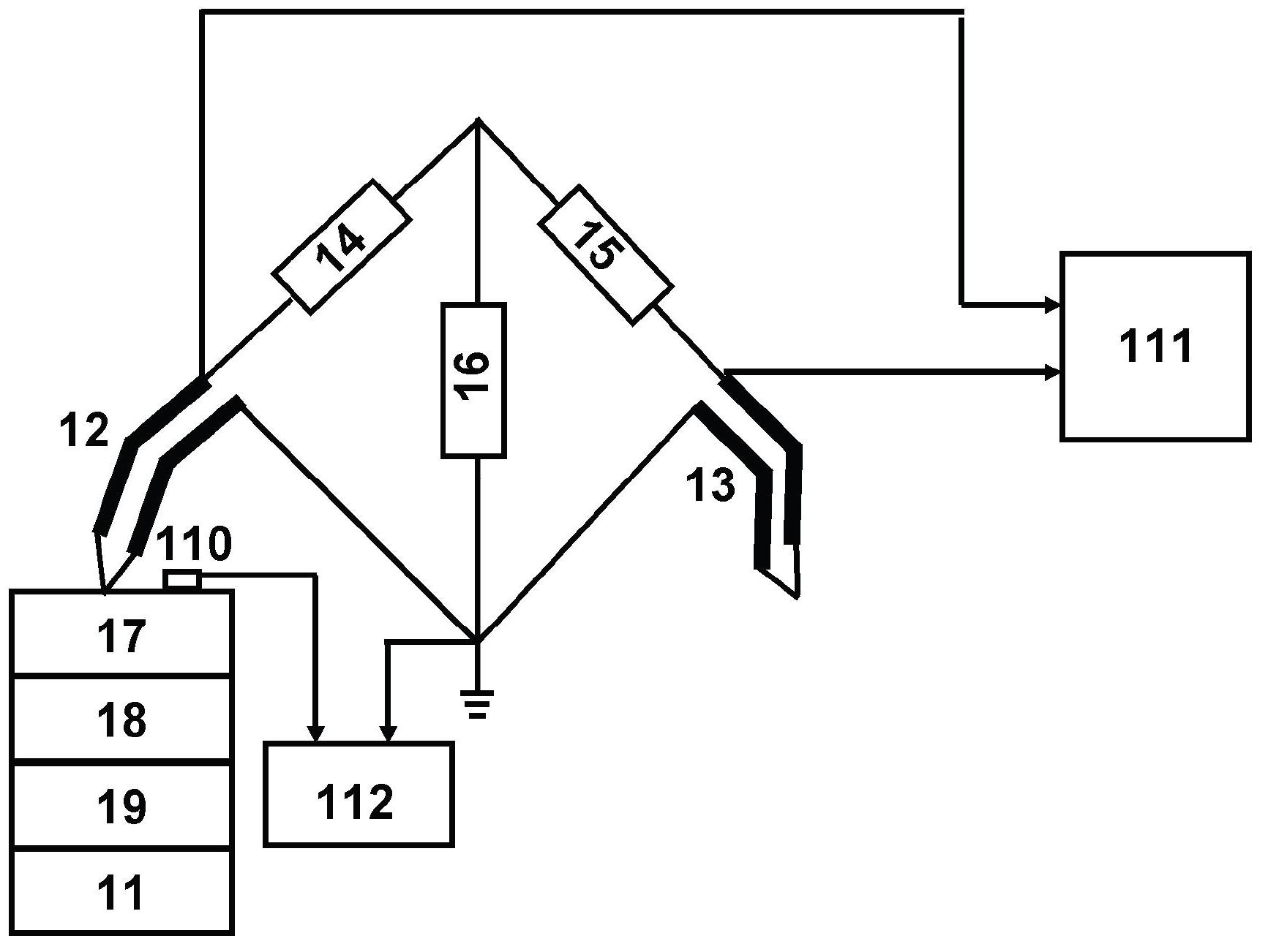
[0048] The nano-thermoelectric multi-parameter in-situ quantitative characterization technology established in this application was used to test the micro-region thermal conductivity of the Bi-Sb-Te thermoelectric thin film, and Figure 6 shows the test results. Among them, Figure 6(a) is the AFM image of the surface topography of the sample, and Figure 6(b) is the micro-area triple frequency of the three measurement points obtained in situ in the corresponding area of ​​the sample by the established nano-thermoelectric multi-parameter in-situ quantitative characterization technique The relationship between the thermal conductance signal and the logarithm of the excitation frequency. According to the near-field thermal imaging conditions, the microscopic thermal conductivity can be calculated as λ=1.668W / (m·K). Since the macroscopic thermal conductivity test technology of thin film has not been satisfactorily resolved so far, it is impossible to compare the thermal conductivity...

Embodiment 2

[0050]The micro-region Seebeck coefficient of the Bi-Sb-Te thermoelectric thin film was tested by applying the nano-thermoelectric multi-parameter in-situ quantitative characterization technology established in this application. Figure 7 shows the test results. It must be pointed out that the results are consistent with those in Figure 8 Results obtained simultaneously in situ during thermoelectric characterization of micro-domains. Figure 7(a) shows the test results of the probe voltage under different excitation voltages, and Figure 7(b) shows the test results of the Seebeck voltage under different excitation voltages. According to the specific thermistor characteristics of the thermal probe and the balance characteristics of the thermoelectric circuit bridge, the temperature of the probe under different excitation voltages can be calculated from Figure 7(a), which corresponds to the temperature of the micro-region of the thermoelectric film. Thus, according to the calculate...


PUM


Abstract

The invention relates to a nano-thermoelectric energy material multi-parameter in-situ quantitative characterization device based on an atomic force microscope, which is used for detecting a micro-area heat conduction coefficient, a Seebeck coefficient and other thermoelectric property parameters of a detected nano-thermoelectric material sample. The device comprises a nano-thermoelectric multi-parameter atomic force microscope in-situ excitation platform and a nano-thermoelectric multi-parameter in-situ detection platform, wherein the nano-thermoelectric multi-parameter atomic force microscope in-situ excitation platform is used for providing a basic hardware platform required in nano-thermoelectric multi-parameter excitation and realizing in-situ simultaneous excitation of a micro-area frequency-tripled heat conduction signal and a micro-area stable-state Seebeck direct current voltage signal of a nano-thermoelectric material; and the nano-thermoelectric multi-parameter in-situ detection platform is used for realizing in-situ real-time detection and data processing of micro-area heat conduction and Seebeck voltage of the nano-thermoelectric material and realizing real-time display of the quantitative characterization results of the micro-area heat conduction coefficient and the Seebeck coefficient. According to the device disclosed by the invention, the nano-detection function of the atomic force microscope, the frequency tripling detection principle of macro-heat conductivity and the test principle of the macro-Seebeck coefficient are combined for establishing a nano in-situ evaluation device which is based on the commercial atomic force microscope and combines the properties of nano-scale heat excitation and thermoelectric multi-parameter detection.

Description

technical field [0001] The application relates to a multi-parameter in-situ quantitative characterization device for nanometer thermoelectric materials based on an atomic force microscope, which belongs to the field of signal detection instruments. Background technique [0002] As an important strategic energy material, thermoelectric materials have very broad application prospects in many important fields such as microelectronics, optoelectronics, deep space exploration, national defense and military industry, and energy conservation and environmental protection. At present, the main obstacle restricting the wide application of thermoelectric materials is their low thermoelectric conversion efficiency. Nanotechnology has opened up a new way for the development of high-performance thermoelectric materials. As a result, nano-thermoelectric materials have become the most active and promising research field in the current international thermoelectric field, and the measurement ...

Claims


Application Information

Patent Timeline
Patent Type & Authority Applications(China)
IPC IPC(8): G01N25/20
CPCG01Q60/58G01N27/00B82Y35/00
Inventor 曾华荣陈立东赵坤宇惠森兴殷庆瑞李国荣
Owner 江苏先进无机材料研究院
Why Eureka
Try Eureka