KTa1-xNbxO3 (KTN) crystal quadratic electro-optical effect-based laser deflection modulation method
A secondary electro-optic and crystal technology, applied in optics, nonlinear optics, instruments, etc., can solve the problems of demanding requirements, increasing the number of electrodes, inconvenient device design, etc., and achieves the effect of facilitating device design and simple sample production
- Summary
- Abstract
- Description
- Claims
- Application Information
AI Technical Summary
Problems solved by technology
Method used
Image
Examples
Embodiment 1
[0024] Example 1: Cu:KTa 0.63 Nb 0.37 o 3 Crystal electro-optical deflection process
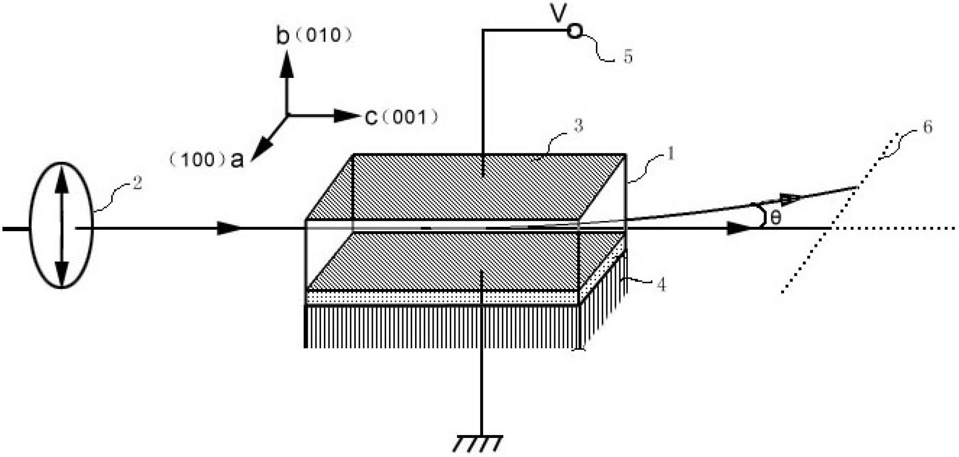
[0025] Such as figure 1 As shown, in this embodiment, we use KTN crystal doped with Cu ions 0.1wt%, Nb content x is 0.37 as the deflection element, the Curie point of the crystal is 20.5°C, and the crystal size a×b×c=3mm×2mm× 6mm, each crystal plane is perpendicular to the crystal axis direction, the metal electrode end face is (010) plane (3mm×6mm), the laser light source is single-biased 532nm green light and single-biased 633nm red light, the beam diameter is 1mm, and the light intensity is 1~2mW.
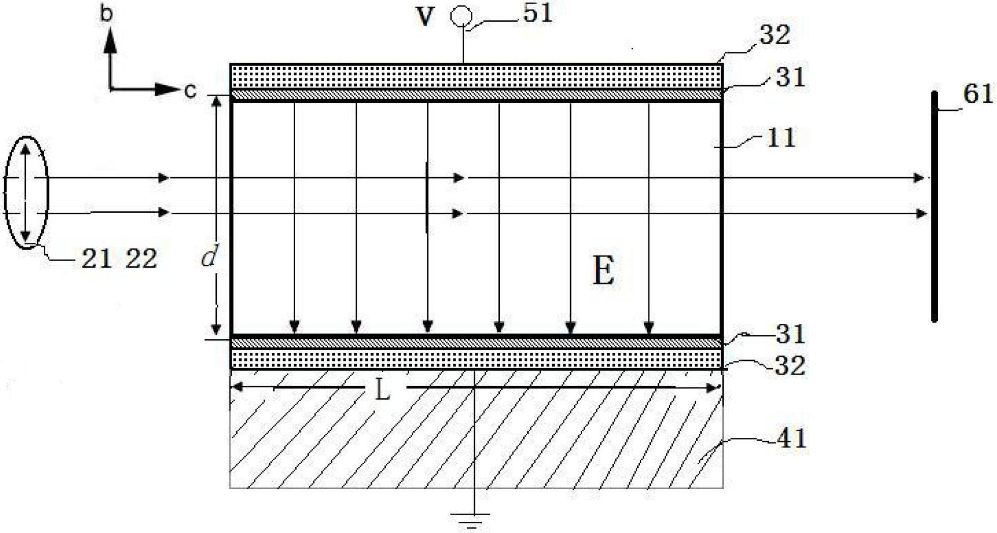
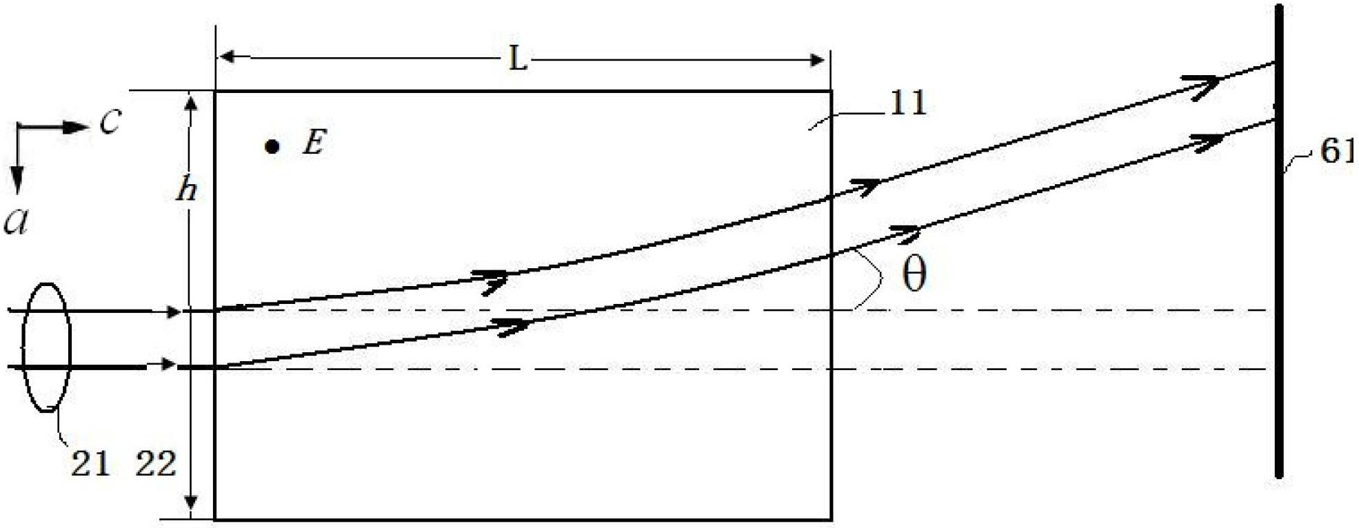
[0026] As shown in Figure 2, the electrode is designed to plate a 50±1nm thick titanium (Ti) metal film on the surface of the crystal (010) by ion sputtering, and then apply silver conductive glue on the surface of the film to enhance the conductivity of the electrode and prevent Ti nano The layer is oxidized; in this electrode design mode, the direction of the electric field E is parallel...
Embodiment 2
[0030] Example 2: Cu:KTa 0.6 Nb 0.4 o 3 Electro-optical deflection process of crystal
[0031] In this embodiment, a KTN crystal doped with Cu ions of 0.2wt% and with an Nb content x of 0.4 is used as the deflection element. (010) surface (2mm×5mm); the electrode is designed to make a 1±0.1um thick aluminum film on the (010) crystal surface by vacuum evaporation, and then coat silver conductive glue on the aluminum film.
[0032] The crystal temperature was controlled at 46±0.2°C during deflection. Other deflection implementation processes are the same as in Embodiment 1. The deflection result of this implementation example is similar to that of Example 1, the difference is that the deflection value is significantly reduced, which is due to the smaller electrode area and light transmission distance, indicating that increasing the electrode area and increasing the light transmission distance can effectively enhance the deflection of the laser.
Embodiment 3
[0033] Example 3: Cu: KTa 0.67 Nb 0.33 o 3 Electro-optical deflection process of crystal
[0034] In this embodiment, a KTN crystal doped with 0.5wt% Cu ions and 0.33 Nb composition is used as the deflection element. The Curie point of the crystal is 4.5°C, and the crystal size a×b×c=3mm×1mm×7mm. Perpendicular to the direction of the crystal axis, the end face of the electrode is a (010) plane (3mm×7mm), and the electrode is made by coating a conductive glue on a 50nm ion-sputtered Pt film. The crystal temperature was controlled at 6±0.2°C during deflection. The implementation process of deflection is the same as that of Embodiment 1.
[0035] The deflection result of this implementation example is similar to that of Example 1, because the electrode end face and light transmission distance are increased, and the crystal thickness is reduced, so the deflection efficiency of the crystal is improved.
[0036] In the present invention, we only use the KTN crystal doped with c...
PUM
| Property | Measurement | Unit |
|---|---|---|
| Curie point | aaaaa | aaaaa |
| Curie point | aaaaa | aaaaa |
| Curie point | aaaaa | aaaaa |
Abstract
Description
Claims
Application Information


