Improved LED chip having current blocking layer and preparation method thereof

A current blocking layer and LED chip technology, applied in circuits, electrical components, semiconductor devices, etc., can solve the problems of uneven current diffusion, low light extraction efficiency, and high heat of LED chips, so as to improve light extraction efficiency, increase reflection probability, The effect of meeting mass production requirements

Inactive Publication Date: 2012-09-26
GUANGDONG TONGFANG ILLUMINATIONS CO LTD
View PDF4 Cites 9 Cited by
  • Summary
  • Abstract
  • Description
  • Claims
  • Application Information

AI Technical Summary

Problems solved by technology

[0003] In view of the problems of high heat generation, uneven current diffusion and low light extraction efficiency of LED chips in the prior art, the purpose of the present invention is to provide a LED chip with high thermal stability, good current diffusion, high light extraction efficiency and mass production LED chip structure and its preparation method

Method used


Image

  • Improved LED chip having current blocking layer and preparation method thereof
  • Improved LED chip having current blocking layer and preparation method thereof
  • Improved LED chip having current blocking layer and preparation method thereof

Examples


Embodiment Construction

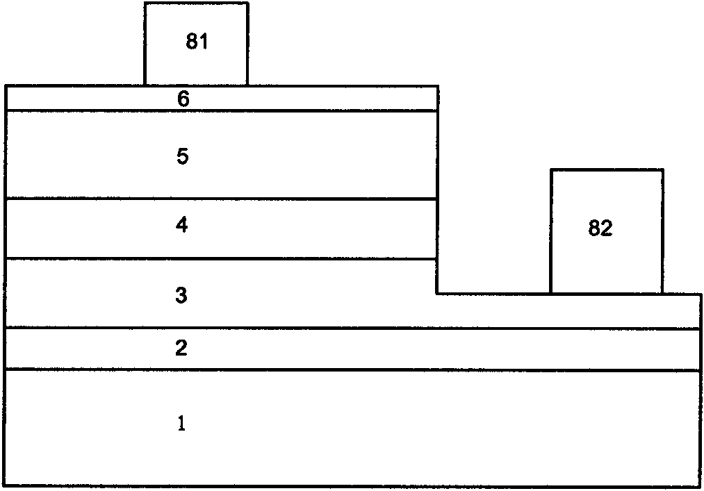
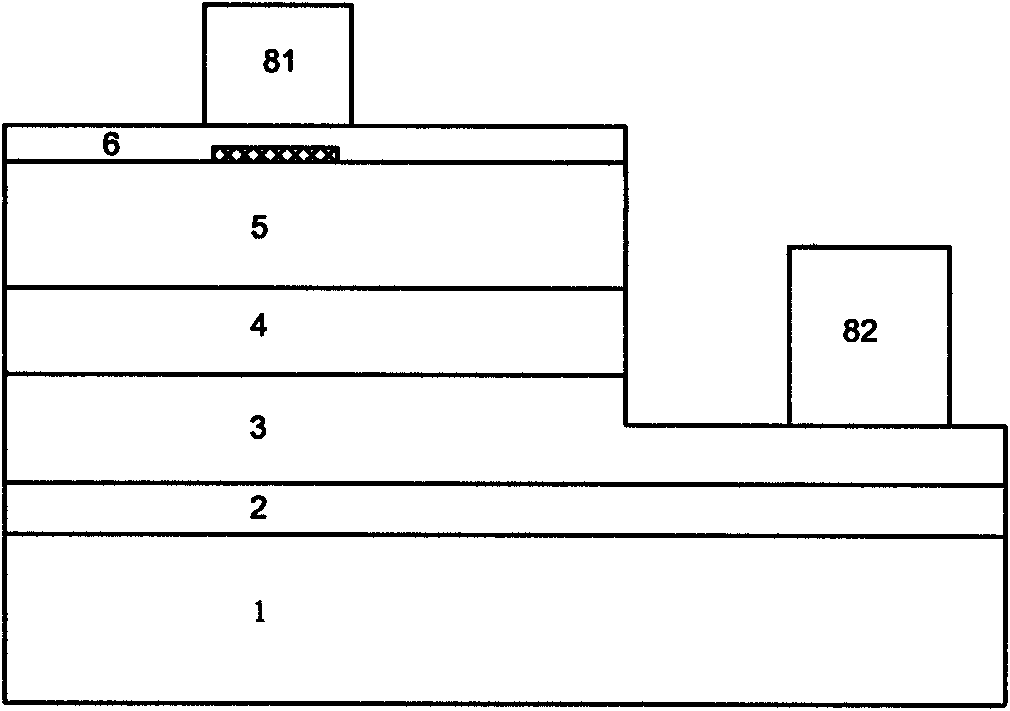
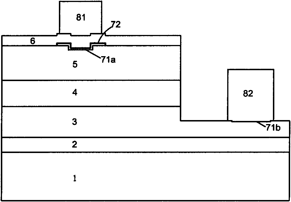
[0031] See image 3 , An improved light-emitting diode chip with a current blocking layer includes: an N-type semiconductor layer 3, a light-emitting layer 4 formed on the N-type semiconductor layer, a P-type semiconductor layer 5 formed on the light-emitting layer, and a P-type semiconductor layer. The transparent conductive layer 6 on the transparent conductive layer, the P electrode 81 formed on the transparent conductive layer, and the N electrode 82 formed on the N-type semiconductor layer. A smooth surface is formed on the P-type semiconductor layer directly below the P-type electrode. A trench 71a, and a current blocking layer 72 is formed on the first trench 71a.

[0032] In actual production, the LED chip further includes a substrate 1 and a buffer layer 2 formed on the substrate as required. The N-type semiconductor layer 3, the light-emitting layer 4, and the P-type semiconductor layer 5 are sequentially formed on the buffer layer 2. on. The addition of the buffer lay...


PUM

PropertyMeasurementUnit
Depthaaaaaaaaaa
Depthaaaaaaaaaa

Abstract

The present invention provides an improved LED chip having a current blocking layer and a preparation method thereof, belonging to the field of semiconductor technology. The LED chip includes a laminated structure of an N type semiconductor layer, a light-emitting layer and a P type semiconductor layer, a transparent conductive layer, a P electrode formed on the transparent conductive layer and an N electrode formed on the N type semiconductor layer. A first groove with a smooth surface is formed at a position corresponding to the P electrode just under the P type semiconductor layer. The current blocking layer is formed on the groove. According to the LED chip provided by the invention, the light-emitting efficiency of the chip is raised and a service life of the chip is prolonged, and the preparation method is simple and convenient and can completely meet a requirement of mass production.

Description

【Technical Field】 [0001] The invention belongs to the technical field of semiconductors, relates to an LED chip structure and a preparation method thereof, and particularly refers to an improved LED chip with a current blocking layer and a preparation method thereof. 【Background technique】 [0002] At present, the structure of light-emitting diode (LED) chips includes a front-mounted structure, a vertical structure and a flip-chip structure. figure 1 As shown, it mainly includes a substrate 1, a buffer layer 2 (buffer layer) formed on the substrate, an N-type semiconductor layer 3 formed on the buffer layer, a light-emitting layer 4 formed on the N-type semiconductor layer, and a light-emitting layer The P-type semiconductor layer 5 on the layer forms the transparent conductive layer 6 on the P-type semiconductor layer 5, and the P electrode 81 and the N electrode 82. Because the current accumulation effect of the LED chip is particularly obvious, that is, the current is mainly c...

Claims


Application Information

Patent Timeline
IPC IPC(8): H01L33/14H01L33/42H01L33/00
Inventor 樊邦扬叶国光梁伏波杨小东曹东兴
Owner GUANGDONG TONGFANG ILLUMINATIONS CO LTD
Why Eureka
Try Eureka