Organic light-emitting diode, display and illuminating device

A technology of light-emitting elements and organic electric fields, which can be applied to organic light-emitting devices, parameters of organic light-emitting devices, lighting devices, etc., and can solve problems such as difficulty in practical use, inability to obtain white light, and low luminous efficiency

Active Publication Date: 2012-09-26
KK TOSHIBA
View PDF4 Cites 16 Cited by
  • Summary
  • Abstract
  • Description
  • Claims
  • Application Information

AI Technical Summary

Problems solved by technology

In this way, various efforts have been made to obtain white light through various adjustments such as the composition of the element and the materials used, but in reality, perfect white light cannot be obtained.
Even if white light is obtained, it is difficult to be practical if the luminous efficiency is low

Method used


Image

  • Organic light-emitting diode, display and illuminating device
  • Organic light-emitting diode, display and illuminating device
  • Organic light-emitting diode, display and illuminating device

Examples


no. 1 Embodiment approach

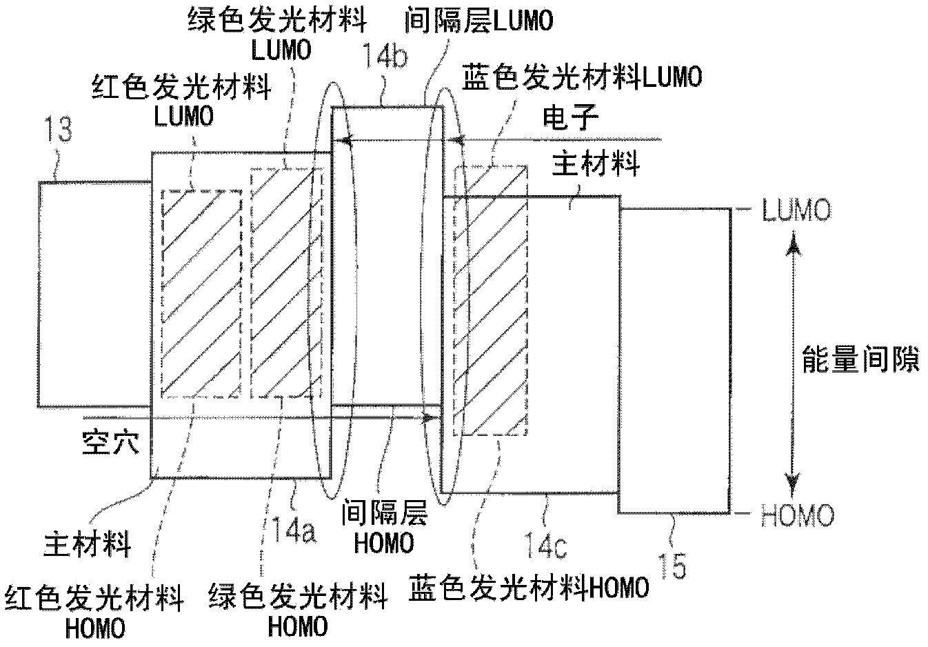
[0022] For the first embodiment of the present invention, refer to figure 2 Be explained. figure 2 It is an energy level diagram of the organic electroluminescence element related to the first embodiment.

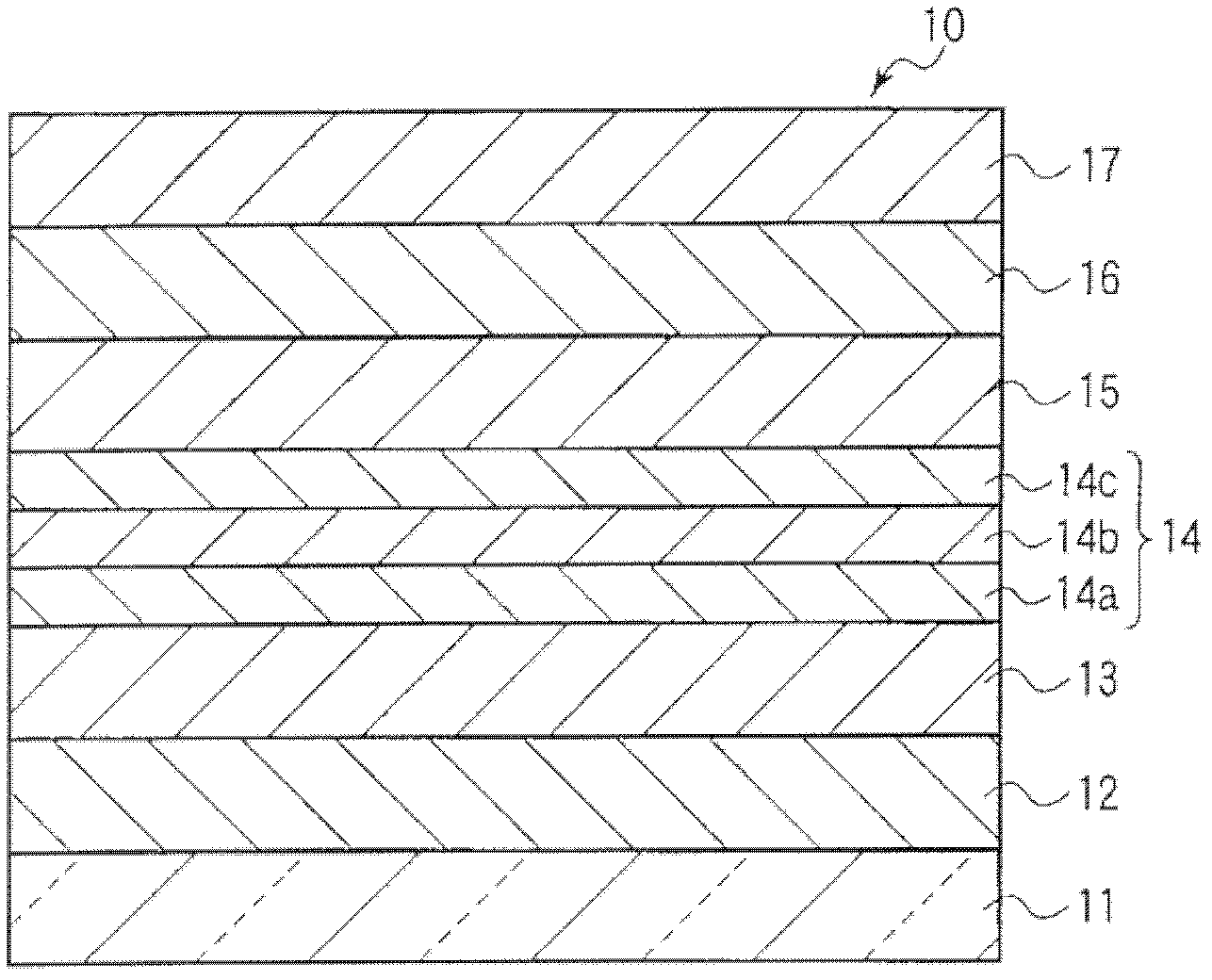
[0023] The red-green light-emitting layer 14a has a structure in which a host material having hole transport properties is doped with a red phosphorescent material and a green phosphorescent material. The blue light-emitting layer 14c has a structure in which a blue fluorescent light-emitting material is doped into an electron-transporting host material.

[0024] The spacer layer 14b has an effect of preventing energy transfer from the blue light-emitting layer 14c to the red-green light-emitting layer 14a, and is made of a hole-transporting material. The hole-transporting material contained in the spacer layer 14b is a single material, and the spacer layer 14b does not contain an electron-transporting material.

[0025] When a voltage is applied to the organic EL elem...

no. 2 Embodiment approach

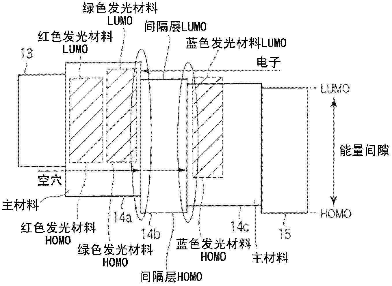
[0049] refer to image 3 A second embodiment of the present invention will be described. image 3 It is an energy level diagram of the organic electroluminescent element according to the second embodiment.

[0050] The red-green light-emitting layer 14a has a structure in which a red phosphorescent material and a green phosphorescent material are doped into a host material having hole transport properties. The blue light-emitting layer 14c has a structure in which a blue fluorescent light-emitting material is doped into a host material having electron transport properties.

[0051] The spacer layer 14b has a function of preventing energy from moving from the blue light-emitting layer 14c to the red-green light-emitting layer 14a, and is made of an electron-transporting material. The electron-transporting material constituting the spacer layer 14b is a single material, and the spacer layer 14b contains a hole-transporting material.

[0052] When a voltage is applied to the o...

Embodiment 1

[0069] A hole-transporting material was used for the spacer layer, and an organic EL device was produced as follows.

[0070] A transparent electrode made of ITO (indium tin oxide) with a thickness of 100 nm was formed as an anode on a glass substrate by vacuum evaporation. As the material of the hole transport layer, α-NPD and TCTA were sequentially deposited by vacuum deposition to form a hole transport layer with a total thickness of 40 nm and 20 nm of 60 nm. As the material of the red-green light-emitting layer, CBP as a bipolar main material, Ir(hflpy)(acac) as a green light-emitting material, and Ir(piq)3 as a red light-emitting material can be used. Control the evaporation rate so that the weight ratio is 69.6:30:0.4, and co-deposit on the hole transport layer using a vacuum evaporation device to form a red-green light-emitting layer with a thickness of 25 nm. The HOMO of the green light-emitting material is 5.2 eV, and the HOMO of the red light-emitting material is 5....


PUM

PropertyMeasurementUnit
thicknessaaaaaaaaaa
porosityaaaaaaaaaa
thicknessaaaaaaaaaa

Abstract

The embodiment of the invention relates to an organic light-emitting diode, and a display and a lighting device using the same. The organic light-emitting diode uses a fluorescent emitting dopant in a blue emissive layer and phosphorescent emitting dopants in a red and green emissive layer, white light emission can be obtained at high luminous efficiency. According to one embodiment, there is provided an organic light-emitting diode (10) including an anode (12) and a cathode (17) which are arranged apart from each other, a red and green emissive layer (14a) on the anode side and a blue emissive layer (14c) on the cathode side, which are arranged to be separated from each other between the anode (12) and the cathode (17), and a spacer layer (14b) which is inserted between the red and green emissive layer (14a) and the blue emissive layer (14c).

Description

[0001] This application is based on Japanese patent application 2011-065040 (filing date: 23 / 03 / 2011), and claims the priority of this Japanese patent application. This application refers to this Japanese Patent Application including its entire contents. technical field [0002] Embodiments of the present invention relate to an organic electroluminescent element, and a display device and a lighting device using the organic electroluminescent element. Background technique [0003] In recent years, organic electroluminescence elements (hereinafter referred to as organic EL elements) used for applications such as planar light sources have attracted attention. The organic electroluminescence element is constituted by sandwiching a light-emitting layer made of an organic material between a pair of electrodes, a cathode and an anode. After voltage is applied to the organic electroluminescent element, electrons are injected from the cathode and holes are injected into the light-em...

Claims


Application Information

Patent Timeline
Patent Type & Authority Applications(China)
IPC IPC(8): H01L51/52H01L51/54C09K11/06H01L27/32H05B33/14
CPCH01L51/5004H01L51/0059H01L2251/5376H01L51/0085H01L51/5044H01L51/0052H10K85/615H10K85/631H10K85/342H10K50/11H10K2101/40H10K50/131H10K2101/27Y02B20/30H10K2101/00H10K2101/30
Inventor 泽部智明高须勋小野富男榎本信太郎金子高志青野伸二郎
Owner KK TOSHIBA
Why Eureka
Try Eureka