

Organic semiconductor device by using alkali metal rubidium compound as buffer layer or electron injection layer
A technology of organic semiconductor and electron injection layer, which is applied in the direction of semiconductor devices, semiconductor/solid-state device manufacturing, electric solid-state devices, etc., can solve the problems of evaporation temperature increase process, unfavorable industrial production, and negative impact on devices, so as to improve injection and transport, balance of electron and hole numbers, effects of increased number of electrons
- Summary
- Abstract
- Description
- Claims
- Application Information
AI Technical Summary
Problems solved by technology
Method used
Image

Examples
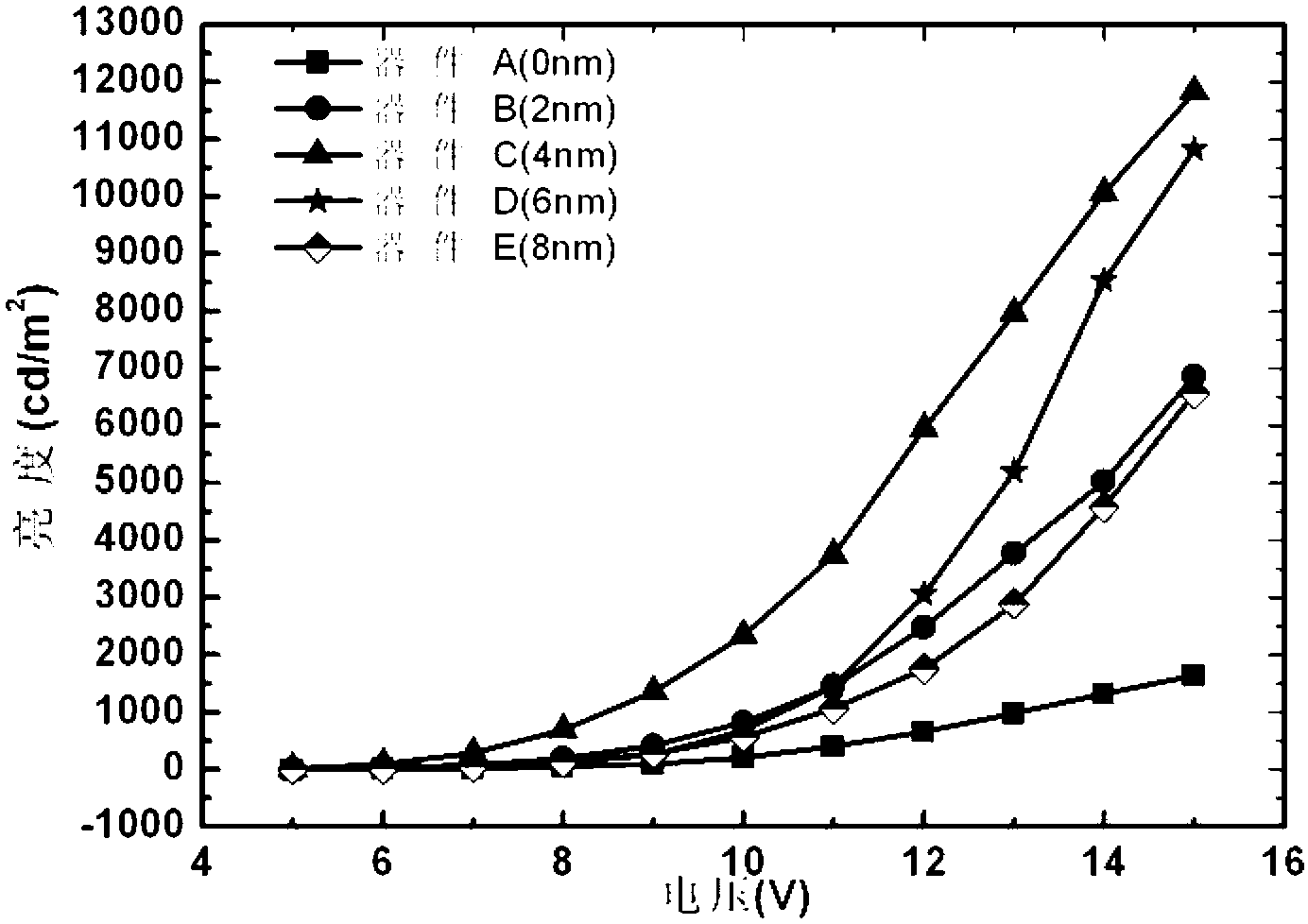
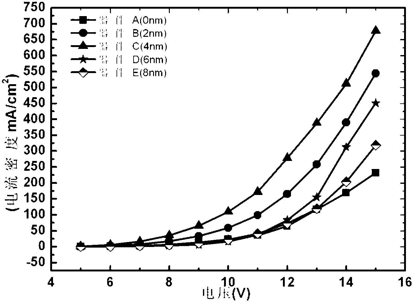
Embodiment 1
[0019] Example 1: Preparation of bottom-emission organic light-emitting devices
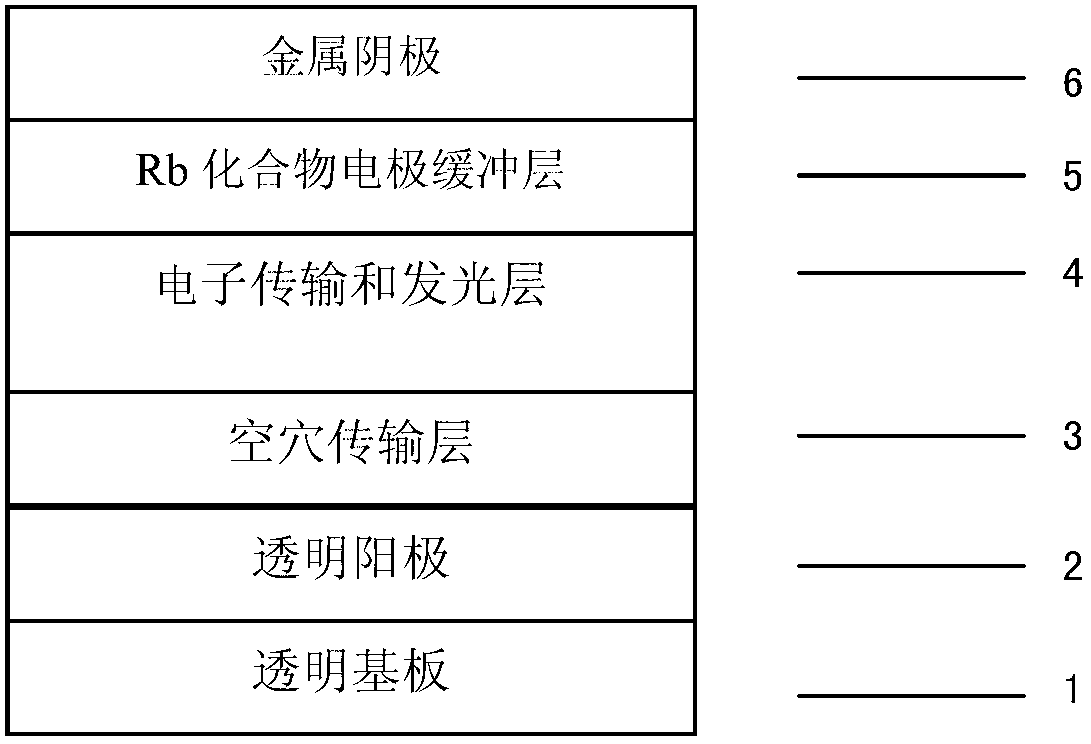
[0020] The process of the present invention for making bottom-emitting organic light-emitting devices: first, clean the ITO glass, then dry it, and then treat it with ultraviolet light for 10 minutes, transfer the ITO substrate to a vacuum evaporation system, and when the vacuum degree reaches 4×10 -4 Pa, the evaporation of the organic layer (including the hole transport layer 3 and the electron transport and light-emitting layer 4, and / or the hole injection layer), the cathode buffer layer (or the organic / Rb doped layer) is carried out, and finally the device is taken out An aluminum electrode is evaporated on it, and the performance of the device is tested after the above-mentioned process is completed.
[0021] In this embodiment, the Rb compound material is introduced into the organic light-emitting device as the cathode buffer layer (or doped layer) material to improve the electron injection...
PUM
 Abstract
Description
Claims
Application Information