Method for forming silicon dioxide spacer with uniform thickness

A silicon dioxide, uniform thickness technology, used in electrical components, semiconductor/solid-state device manufacturing, circuits, etc., to solve problems such as film thickness uniformity differences

Inactive Publication Date: 2012-10-10
SHANGHAI HUALI MICROELECTRONICS CORP
View PDF4 Cites 1 Cited by
  • Summary
  • Abstract
  • Description
  • Claims
  • Application Information

AI Technical Summary

Problems solved by technology

In this way, in the case of the same increase in thickness, the film thickness uniformity of the two regions will have a huge difference

Method used


Image

  • Method for forming silicon dioxide spacer with uniform thickness
  • Method for forming silicon dioxide spacer with uniform thickness
  • Method for forming silicon dioxide spacer with uniform thickness

Examples


Embodiment Construction

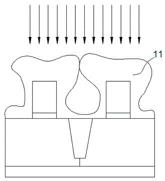
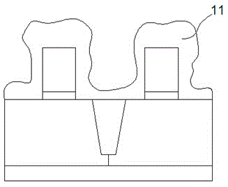
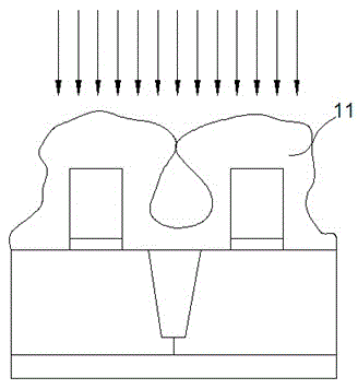
[0015] The invention provides a method for forming silicon dioxide sidewalls with uniform thickness. First, a layer of sidewall oxide layer is deposited on the surface of a plurality of gate devices; the formed sidewall oxide layer is etched to make the device The seal at the gate is opened; a sidewall oxide layer is deposited on the previously formed sidewall oxide layer, and the formed sidewall oxide layer is etched again; the above deposition and etching process of the sidewall oxide layer are repeated , until the thickness of the formed sidewall oxide layer reaches the target thickness.

[0016] The method provided by the present invention will be further described in detail through the following examples, so as to better understand the content of the present invention, but the content of the examples does not limit the protection scope of the present invention.

[0017] In the present invention, the silicon dioxide layer 11 is deposited at a low temperature. As the deposi...


PUM


Abstract

The invention provides a method for forming a silicon dioxide spacer with uniform thickness. The method comprises the following steps of: firstly, depositing a spacer oxidation layer on a surface of a device on which a plurality of grids are formed; etching the formed spacer oxidation layer to enable a sealing port formed between two grids of the device in the deposition process to be opened; depositing a spacer oxidation layer on the formed spacer oxidation layer; secondarily etching the formed spacer oxidation layer; and repeating the depositing and etching processes of the spacer oxidation layer until the thickness of the formed spacer oxidation layer reaches a target thickness, wherein the etching is realized by using far-end NF3+NH3 plasma.

Description

technical field [0001] The invention relates to the field of integrated circuit manufacturing, in particular to a method for forming silicon dioxide sidewalls with uniform thickness on the device surface. Background technique [0002] Spacer is a necessary structure in the industry to manufacture semiconductor CMOS devices. It can not only protect the gate, but also reduce the short channel effect well with the shallow doping (LDD) process. [0003] So far, the traditional sidewall process mostly uses a composite layer of silicon dioxide and silicon nitride (silicon nitride is the outer layer). When it comes to the 65nm process and below, the requirements for the deposition of silicon dioxide films are getting more and more High, not only requires a low temperature deposition process (<300~600°C), but also requires good uniformity, especially for different areas (large line width, such as a single polycrystalline gate area and small line width, such as static memory The ...

Claims


Application Information

Patent Timeline
IPC IPC(8): H01L21/8238
Inventor 张文广陈玉文
Owner SHANGHAI HUALI MICROELECTRONICS CORP
Why Eureka
Try Eureka