Supercharge Your Innovation With Domain-Expert AI Agents!

Substrate of active matrix/organic light emitting diode (AMOLED) device and mask plates of substrate

A mask plate and substrate technology, which is applied in the manufacture of electrical solid devices, semiconductor devices, semiconductor/solid state devices, etc., can solve problems such as color errors and mask plate error alignment, and achieve the effect of improving panel quality

Inactive Publication Date: 2012-10-24
SICHUAN CCO DISPLAY TECH
View PDF8 Cites 2 Cited by
  • Summary
  • Abstract
  • Description
  • Claims
  • Application Information

AI Technical Summary

Problems solved by technology

The substrates of AMOLED devices currently used in the evaporation process such as figure 1 As shown, the mask is as figure 2 As shown, the R, G, B pixel ITO (light-emitting part) and TFT pixel circuit (non-light-emitting part) of the substrate are arranged vertically in sequence, and the mask plate adopts a matching structure, generally as follows figure 2 The strip-shaped mask plate shown has a relatively long hole in the middle of the mask plate. The substrate and mask plate of this structure are only suitable for the substrate evaporation of small-sized AMOLED devices. For large-sized substrates, because The metal pattern of the mask plate is thin, so when the mask plate is used on the evaporation equipment, the center of the mask plate sinks a little more than the edge, and this sinking phenomenon will cause the misalignment of the mask plate in the organic evaporation process. , causing the organic substances to be stacked on each other, which causes the color mixing of the substrate of the AMOLED device, which will cause the wrong color of the display

Method used


Image

  • Substrate of active matrix/organic light emitting diode (AMOLED) device and mask plates of substrate
  • Substrate of active matrix/organic light emitting diode (AMOLED) device and mask plates of substrate
  • Substrate of active matrix/organic light emitting diode (AMOLED) device and mask plates of substrate

Examples


Embodiment Construction

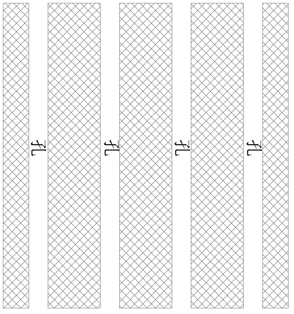
[0011] The structure of the substrate of the AMOLED device of the present invention is as image 3 As shown, its R, G, B pixel ITO and TFT pixel circuits adopt a symmetrical arrangement structure in pairs, so it can ensure that the TFT circuit part that does not need evaporation has the advantage of a wider area, such as Figure 4 As shown, the pixel structure of the substrate is changed, and a wider connection bridge is placed on the corresponding part of the wider TFT pixel circuit, so a mask plate that is more efficient than the existing mask plate can be manufactured. Compared with the existing hole-digging structure with a longer arrangement of mask plates, the mask plate with a shorter arrangement of hole-digging structures in the present invention can effectively improve the deformation of the mask plate.

[0012] In addition, the present invention arranges metal wires on the region of the TFT pixel circuit, and utilizes the metal wires to vapor-deposit organic matter, ...


PUM


Abstract

The invention provides a substrate of an active matrix / organic light emitting diode (AMOLED) device, which can solve the alignment problem and color mixing problem in evaporation, and mask plates of the substrate. The substrate of the AMOLED device comprises a red (R), green (G) and blue (B) pixel indium tin oxide (ITO) and thin film transistor (TFT) pixel circuit, and the R, G, B pixel ITO and TFT pixel circuit adopts a symmetric arrangement structure that every two circuits depends on each other. Since the mask plates are interconnected with each other by bridging and have a short arrangement perforated structure, the deformation phenomenon of the mask plates in an organic matter evaporation step can be prevented, simultaneously the organic matters can be correctly evaporated, and the purpose for improving the panel quality can be achieved.

Description

technical field [0001] The invention relates to a manufacturing process of an AMOLED device, in particular to a substrate of an AMOLED device and a mask plate thereof. Background technique [0002] The manufacturing process of AMOLED (Active Matrix / Organic Light Emitting Diode active matrix organic light emitting diode panel) device is divided into: substrate process, evaporation process and packaging process. The substrate process is to generate TFT (Thin Film Transistor thin film transistor) on the glass, and silicon material and metal material can be laminated. In order to light up the panel by using the TFT formed through the substrate process, it is necessary to perform an organic substance vapor deposition process on the TFT substrate. The organic substance vapor deposition process is to vapor-deposit the vaporized organic substance on the TFT substrate. The substrates of AMOLED devices currently used in the evaporation process such as figure 1 As shown, the mask is ...

Claims


Application Information

Patent Timeline
IPC IPC(8): H01L27/12H01L21/027C23C14/04
Inventor 金正学洪宣杓
Owner SICHUAN CCO DISPLAY TECH
Features
  • R&D
  • Intellectual Property
  • Life Sciences
  • Materials
  • Tech Scout
  • Unparalleled Data Quality
  • Higher Quality Content
  • 60% Fewer Hallucinations
Learn More