Organic EL device manufacture method

A technology of EL devices and manufacturing methods, applied in semiconductor/solid-state device manufacturing, electric solid-state devices, semiconductor devices, etc., can solve problems such as reduced vacuum degree, blurred images, and reduced yield or productivity, so as to reduce dust or gas , high productivity, and the effect of reducing deflection

Inactive Publication Date: 2012-10-24
HITACHI HIGH-TECH CORP
View PDF2 Cites 3 Cited by
  • Summary
  • Abstract
  • Description
  • Claims
  • Application Information

AI Technical Summary

Problems solved by technology

However, the reflective optical system has the following problems, and there is a problem that it cannot be positioned with good accuracy
(1) Since halo is caused by mirror finishing on the surface of the mask, the illumination intensity cannot be increased, and metal parts cannot be detected if it is lowered.
(2) In order not to damage the substrate surface during positioning, it is necessary to provide a gap of about 0.5mm between the mask and the reflective optical system, and the image becomes blurred due to the reduced depth of field
[0009] Secondly, in the method disclosed in Patent Document 1, since the entire mechanism for positioning the substrate and the mask is placed in a vacuum, dust and heat accompanying the movement of the drive unit or the like may be generated or may be emitted from the drive unit. The gas from the wiring, the gas from the lubricant, and the gas from the surface of the component reduce the vacuum degree
First, the dust that goes into the vacuum adheres to the substrate and the mask and causes poor deposition. Second, the thermal expansion of the mask caused by heat generation changes the deposition specifications. Third, the gas reduces the degree of vacuum. Therefore, there is a problem that the yield rate, that is, the productivity, decreases.
[0010] In addition, since the entire mechanism for positioning the substrate and the mask is installed in a vacuum, if a failure occurs in the drive unit, etc., it will take time to repair and the operating efficiency of the device will decrease.

Method used


Image

  • Organic EL device manufacture method
  • Organic EL device manufacture method
  • Organic EL device manufacture method

Examples


Embodiment Construction

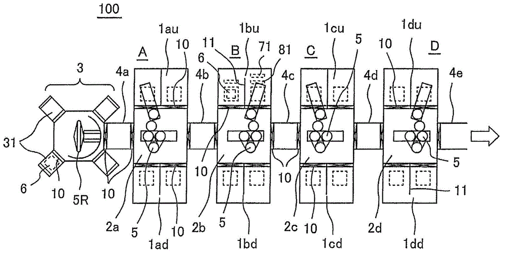
[0076] use figure 1 A first embodiment of the present invention will be described. The organic EL device manufacturing device does not only form a light-emitting material layer (EL layer) and sandwich it with electrodes. Instead, various materials are made into thin films, and a hole injection layer or transport layer is formed on the anode, and a hole injection layer or transport layer is formed on the cathode. Form a multilayer structure such as an electron injection layer or a transport layer, and clean the substrate. figure 1 An example of this manufacturing apparatus is shown.

[0077] The organic EL device manufacturing apparatus 100 of this embodiment roughly includes: the load harness 3 carrying the substrate 6 to be processed; (Sealing process) between six transfer chambers. In this embodiment, the vapor deposition surface of the substrate is conveyed as the upper surface, and the substrate is stood up and vapor deposited during vapor deposition.

[0078]The loa...


PUM


Abstract

The invention provides an organic EL device manufacture apparatus or deposition apparatus that can reduce affection of flexing of substrate and mask or warping of shadow mask, can reduce the generation of powder dust and gas in the vacuum by high precision deposition or configuring the drive part at the atmosphere side, and has high production character, high maintenance character and high work efficiency. Also provided is an alignment device and alignment method that can perform high precision positioning. The invention is characterized in that: firstly, the shadow mask is in contraposition to the substrate in a dependent pose to deposit the deposition material on the substrate; secondly, a permeation type using the light incident on the positioning through hole arranged on the shadow mask to perform positioning; and thirdly, the deposition is performed by reducing the warping of the shadow mask.

Description

[0001] This application was submitted on December 14, 2009, and the application number is 200910253190.7. It is an invention application titled "Organic EL device manufacturing device, film forming device and film forming method, liquid crystal display substrate manufacturing device, positioning device and positioning method" divisional application. technical field [0002] The present invention relates to an organic EL device manufacturing device, a film forming device and a film forming method thereof, a liquid crystal display substrate manufacturing device, a positioning device and a positioning method, and in particular to an organic EL device manufacturing device, a film forming device and a liquid crystal display device suitable for positioning a large substrate. Displays the substrate manufacturing equipment. Background technique [0003] As a powerful method for manufacturing an organic EL device, there is a vacuum evaporation method. The vacuum evaporation method r...

Claims


Application Information

Patent Timeline
Patent Type & Authority Applications(China)
IPC IPC(8): H01L51/00H01L21/68
CPCC23C16/042
Inventor 弓场贤治韭泽信广落合行雄
Owner HITACHI HIGH-TECH CORP
Why Eureka
Try Eureka