Charging method in monocrystalline silicon ingot casting, and monocrystalline silicon ingot casting method

A single crystal silicon and ingot casting technology is applied in the field of single crystal silicon ingot and single crystal silicon ingot charging, which can solve the problems of easy-to-melt single crystal ingot casting process and difficult control of seed crystals.

Active Publication Date: 2012-10-31
JIANGXI SAI WEI LDK SOLAR HI TECH CO LTD
View PDF10 Cites 23 Cited by
  • Summary
  • Abstract
  • Description
  • Claims
  • Application Information

AI Technical Summary

Problems solved by technology

In view of this, the prior art proposes the use of directional solidification to produce monocrystalline silicon, that is, the monocrystalline ingot method, thereby improving the conversion efficiency of crystalline silicon and improving production efficiency to reduce production costs. However, in the prior art, monocrystalline silicon In the crystal ingot casting method, since there are gaps between the seed crystals and between the seed crystals and the crucible wall when the silicon material is loaded, molten silicon will pass between the seed crystals and between the seed crystals and the crucible wall when the silicon raw material is melted. Seed crystals float and melt due to the infiltration of the gaps between them; at the same time, the existing charging method will cause the molten silicon to contact the seed crystals too quickly, resulting in the easy melting of the seed crystals, making it difficult to control the single crystal ingot casting process

Method used


Image

  • Charging method in monocrystalline silicon ingot casting, and monocrystalline silicon ingot casting method
  • Charging method in monocrystalline silicon ingot casting, and monocrystalline silicon ingot casting method

Examples


Embodiment Construction

[0030] The technical solutions in the embodiments of the present invention will be clarified below with reference to the accompanying drawings in the embodiments of the present invention.

[0031] clearly and completely, it is obvious that the described embodiments are only a part of the embodiments of the present invention, not

[0032] All examples. Based on the embodiments of the present invention, those of ordinary skill in the art do not create

[0033] All other embodiments obtained under the premise of sexual labor fall within the protection scope of the present invention.

[0034] In order to make the objects, technical solutions and advantages of the present invention more clearly understood, the present invention is hereinafter described with reference to the accompanying drawings.

[0035] The following examples are described in further detail.

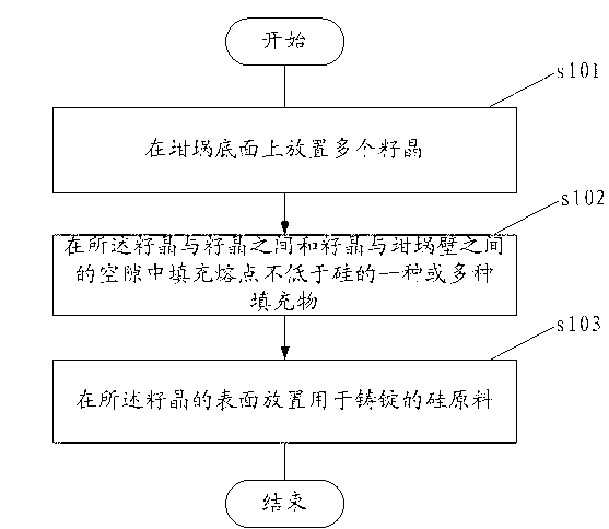
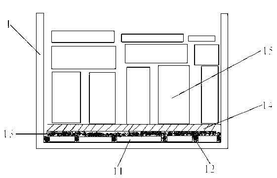
[0036] refer to figure 1 It is a flow chart of the charging method of the single crystal silicon ingot according to t...


PUM


Abstract

The invention discloses a charging method in monocrystalline silicon ingot casting. The method comprises the steps that: a plurality of seed crystals are placed on a bottom surface of a crucible; one or more filling materials with a melting point no lower than that of silicon is filled in gaps among the seed crystals and between the seed crystals and a crucible wall; and a silicon raw material used in ingot casting is placed on the surface of the seed crystals. The invention also provides a monocrystalline silicon ingot casting method. With the method, when the silicon raw material is filled into the crucible, the filling materials with the melting point no lower than that of silicon is filled in gaps among the seed crystals and between the seed crystals and the crucible wall. Therefore, when the silicon raw material is molten, the molten silicon is prevented from entering the gaps among the seed crystals and between the seed crystals and the crucible wall, so that seed crystal floating and melting caused by the molten silicon are prevented. According to the value of silicon raw material thermal conductivity, a leveled charging method is adopted, so that temperature gradient during a monocrystalline silicon ingot casting procedure is increased. Therefore, molten silicon is prevented from contacting the seed crystals in a premature stage, and seed crystals can be prevented from melting too fast. Therefore, difficulty in controlling monocrystalline silicon ingot casting process can be prevented.

Description

technical field [0001] The invention relates to the field of photovoltaics, in particular to a method for charging a single crystal silicon ingot and a method for casting a single crystal silicon ingot. Background technique [0002] The current methods for obtaining the crystalline silicon generally include the Czochralski (CZ, Czochralski) method and the Float-Zone (FZ, Float-Zone) method of single crystal silicon, and the directional solidification method of polycrystalline silicon. Among them, the directional solidification method for producing polysilicon produces large polysilicon ingots each time, which greatly improves the production efficiency. However, due to the defects of grain boundaries and dislocations in conventional polysilicon, this will lead to the conversion of cells produced using this polysilicon. Low efficiency. The cells produced by monocrystalline silicon do not have the above-mentioned low conversion efficiency of polycrystalline silicon, and the co...

Claims


Application Information

Patent Timeline
Patent Type & Authority Applications(China)
IPC IPC(8): C30B11/00C30B29/06
Inventor 胡动力何亮钟德京张涛
Owner JIANGXI SAI WEI LDK SOLAR HI TECH CO LTD
Why Eureka
Try Eureka