Vertical deposition furnace tube
A deposition furnace and vertical technology, applied in the field of vertical deposition furnace tubes, can solve the problems of high cost of silicon dioxide film, unfavorable cost control, etc., and achieve the effect of uniform thickness and improved uniformity
- Summary
- Abstract
- Description
- Claims
- Application Information
AI Technical Summary
Problems solved by technology
Method used
Image

Examples
Embodiment Construction
[0027] In order to make the above objects, features and advantages of the present invention more comprehensible, specific implementations of the present invention will be described in detail below in conjunction with the accompanying drawings.
[0028] In the following description, many specific details are set forth in order to fully understand the present invention, but the present invention can also be implemented in other ways than those described here, so the present invention is not limited by the specific embodiments disclosed below.
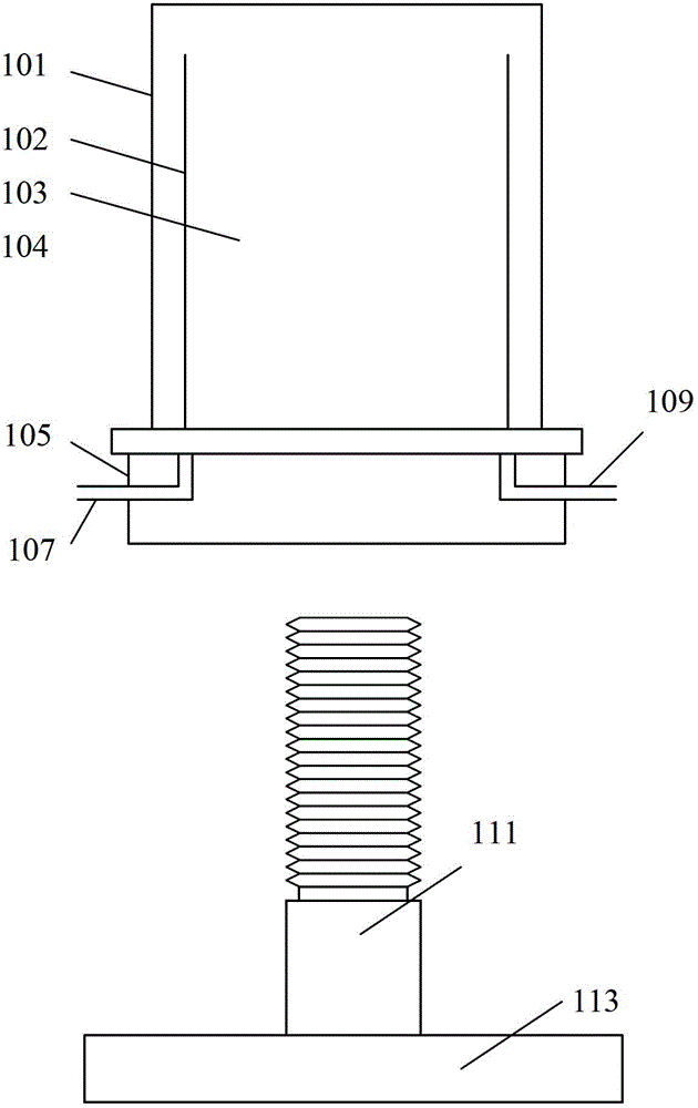
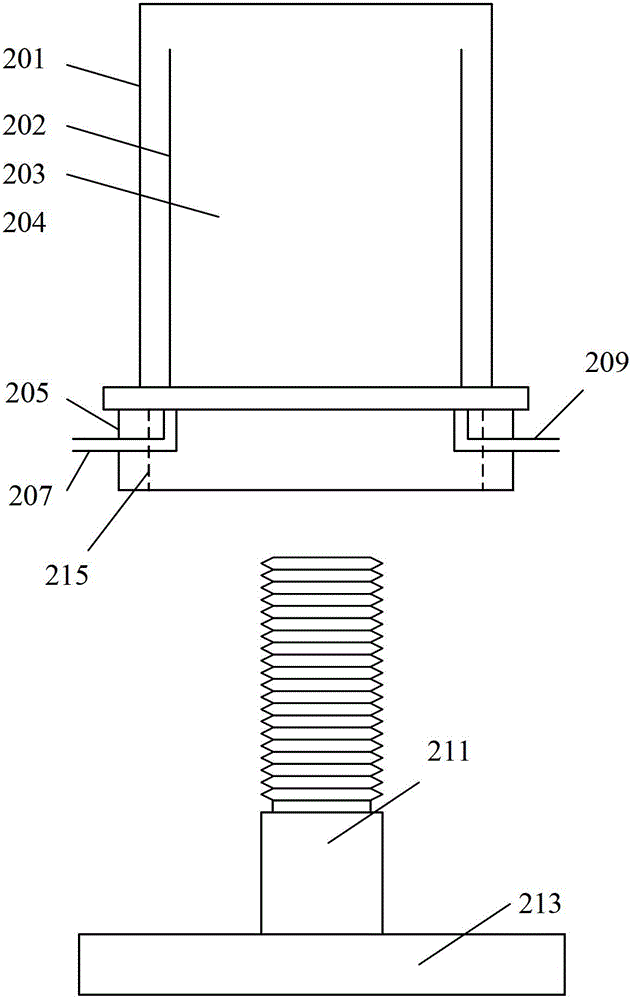
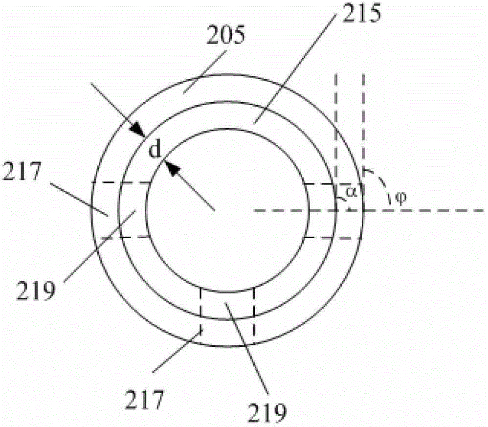
[0029] As mentioned in the background section, the thickness of SiO2 film formed on the wafer near the bottom of the vertical deposition furnace tube in the existing vertical deposition furnace tube was compared with the thickness of the silicon dioxide film formed on the wafer in other positions (middle or top). In contrast, the uniformity is poor, and the method of increasing the distance between the wafers by reducing the number of wafe...
PUM
| Property | Measurement | Unit |
|---|---|---|
| thickness | aaaaa | aaaaa |
Abstract
Description
Claims
Application Information
 - R&D
- Intellectual Property
- Life Sciences
- Materials
- Tech Scout
- Unparalleled Data Quality
- Higher Quality Content
- 60% Fewer Hallucinations
Browse by: Latest US Patents, China's latest patents, Technical Efficacy Thesaurus, Application Domain, Technology Topic, Popular Technical Reports.
© 2025 PatSnap. All rights reserved.Legal|Privacy policy|Modern Slavery Act Transparency Statement|Sitemap|About US| Contact US: help@patsnap.com