JTAG (joint test action group) main controller and realization method of JTAG main controller

A technology of main controller and implementation method, applied in the electronic field, can solve the problems of unable to generate high-frequency test clock, affecting test effect, and large delay

Active Publication Date: 2012-11-14
CAPITAL MICROELECTRONICS
View PDF5 Cites 4 Cited by
  • Summary
  • Abstract
  • Description
  • Claims
  • Application Information

AI Technical Summary

Problems solved by technology

[0007] Traditional JTAG master controllers are implemented by MIPS, ARM and other processors. Since the functions executed by MIPS and ARM systems are implemented by software, and MIPS and ARM’s own instructions are used to complete specific functions, a JTAG instruction needs Use multiple MIPS instructions to simulate, and because the completion of tasks in MIPS and ARM systems is c

Method used


Image

  • JTAG (joint test action group) main controller and realization method of JTAG main controller
  • JTAG (joint test action group) main controller and realization method of JTAG main controller
  • JTAG (joint test action group) main controller and realization method of JTAG main controller

Examples


Embodiment Construction

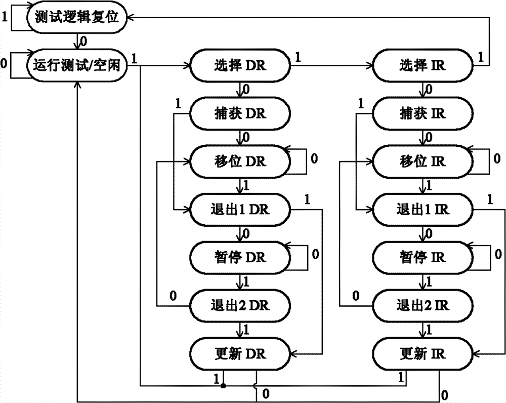
[0019] Figure 4 It is a schematic diagram of the working principle of the JTAG main controller of an embodiment of the present invention.

[0020] This JTAG main controller comprises external NVM410, memory control module 420, clock module 430, embedded memory 440, JTAG signal generator 450; Wherein, memory control module 420, clock module 430, embedded memory 440, JTAG signal generator 450 Integrated on a chip, such as FPGA or ASIC chip.

[0021] When the JTAG main controller is working, it needs to be connected to the target chip 460 through the JTAG signal generator 450 to implement operations such as testing, debugging or emulation of the target chip 460 . The target chip 460 includes a standard JTAG interface, which complies with the IEEE1149.1 standard.

[0022] Figure 4 Among them, the external NVM 410 is used to store HOST instructions from the host 470. The external NVM 410 can be any existing non-volatile memory, such as EEPROM (Electrically Erasable Programmab...


PUM


Abstract

The invention relates to a JTAG (joint test action group) main controller and a realization method of the JTAG main controller. The JTAG main controller comprises a JTAG signal generator. The JTAG signal generator obtains external HOST instructions, in addition, the HOST instructions are analyzed to obtain IR (instruction register) instructions or DR (data register) data, so corresponding JTAG interface signals are generated according to IR instructions or DR data, and a target chip is driven through the JTAG interface signals. The JTAG main controller and the realization method have high execution instruction efficiency, and can be applied into a JTAG device.

Description

technical field [0001] The invention relates to the field of electronics, in particular to JTAG devices. Background technique [0002] As an interface standard of IEEE, JTAG interface plays an important role in the testing, simulation, debugging and other aspects of integrated circuits. Most existing advanced devices support the JTAG protocol, such as DSP, FPGA and other devices. [0003] The standard JTAG interface includes a test clock input signal TCK, a test data input signal TDI, a test mode selection signal TMS, a test data output port TDO, and an optional test reset input signal TRST. [0004] The internal logic of the JTAG device is realized by a TAP state machine, figure 1 A schematic diagram of the state transition of the TAP state machine of the JTAG device specified in the IEEE1149.1 standard is shown. Such as figure 1 As shown, the TAP state machine includes two branches, namely a command register access (IR Access) branch and a data register access (DR Acce...

Claims


Application Information

Patent Timeline
IPC IPC(8): G01R31/28
Inventor 李大伟朱建彰王强王潘丰邹丽娜
Owner CAPITAL MICROELECTRONICS
Why Eureka
Try Eureka