Electrode tape, solar cell module and methods for manufacturing the same

A technology for solar cells and electrode tapes, applied to conductive materials, circuits, adhesives, etc. dispersed in non-conductive inorganic materials, can solve problems such as microcracks on the surface of crystalline silicon

Inactive Publication Date: 2012-11-21
NEO SOLAR POWER CORP
View PDF6 Cites 5 Cited by
  • Summary
  • Abstract
  • Description
  • Claims
  • Application Information

AI Technical Summary

Problems solved by technology

Due to the high temperature of the traditional welding process, thermal stress will be generated between the metal electrode and the crystalline silicon substrate due to different expansion / contraction coefficients, resulting in the disadvantage of micro cracks (Micro Crack) on the crystalline silicon surface

Method used


Image

  • Electrode tape, solar cell module and methods for manufacturing the same
  • Electrode tape, solar cell module and methods for manufacturing the same
  • Electrode tape, solar cell module and methods for manufacturing the same

Examples


Embodiment Construction

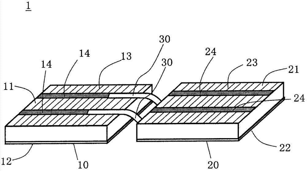
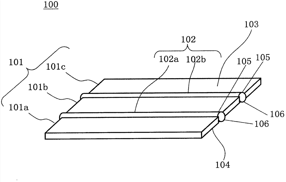
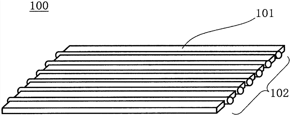
[0158] Embodiments of the present invention will be described below by way of example with reference to the accompanying drawings. The components shown in the drawings do not represent the actual size of the components, and their thickness, width, or length, etc. are drawn exaggeratedly for the sake of illustration. Meanwhile, in all the drawings, the same component symbols represent the same components.

[0159] In this specification, "electrode tape" refers to a tape having electrodes on its structure. "Electrode" refers to an electrically conducting structure. "Tape" means a film (Film), strip (Strip), sheet (sheet) and other similar materials including adhesive materials, usually continuously rolled into a bundle (roll) for storage, but can also be cut into pieces if necessary. After appropriate length, stack and store, or store in other appropriate ways. At normal temperature, the surface of this film can be sticky or non-sticky. A film on a non-sticky surface at room...


PUM


Abstract

An electrode tape and a method for manufacturing the same are disclosed. The electrode tape includes an adhesive film and a conductive structure. The adhesive film includes a first adhesive surface and a second adhesive surface which faces an opposite direction to the first adhesive surface. The conductive structure is embedded in the adhesive film with a first contact point exposed on the first adhesive surface and a second contact point exposed on the second adhesive surface. The cell module comprises the first solar cell and the second solar cell, which can be adhered to each other by using the electrode tape.

Description

technical field [0001] The invention relates to an electrode adhesive tape and a solar battery module, in particular to a double-sided adhesive and double-sided conductive electrode adhesive tape and a solar battery module. Background technique [0002] Solar cells use the photoelectric conversion effect to convert sunlight into electrical energy, which is a clean energy source without pollution. At present, solar cells have been extensively researched and produced, and gradually began to replace traditional electricity. [0003] Common solar cells are semiconductor components including n-p junctions, such as monocrystalline silicon, polycrystalline silicon, amorphous silicon or other thin film semiconductor components with n-p junctions. The n-p junction is usually fabricated by doping n-type or p-type ions into the interior of the semiconductor device by means of diffusion or ion implantation. When light is irradiated to a semiconductor component, electrons and holes of ...

Claims


Application Information

Patent Timeline
IPC IPC(8): C09J7/02H01L31/05H01L25/04H01L31/18C09J7/10
CPCC09J2203/322H01L31/0508H01R4/04C09J2201/602H01B1/22C09J2201/32H01L31/0512Y02E10/50C09J2201/28C09J9/02C09J7/00Y10T428/14Y10T428/1471Y10T428/1438Y10T428/28Y10T428/1443C09J7/10C09J2301/206C09J2301/204C09J2301/314
Inventor 林晴煌梁荣昌蔡佩苍
Owner NEO SOLAR POWER CORP
Why Eureka
Try Eureka