Infrared optical window with double-sided anti-reflection structure
An infrared optical window and anti-reflection technology, applied in the field of infrared optical windows, can solve the problems of low transmittance, achieve the effect of increasing transmittance, improving sensitivity, and simple preparation process
- Summary
- Abstract
- Description
- Claims
- Application Information
AI Technical Summary
Problems solved by technology
Method used
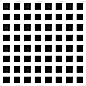
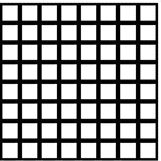
Image

Examples
Embodiment 1
[0027] Step 1, silicon wafer surface treatment: use acetone to ultrasonically clean the double-sided polished silicon wafer, then rinse it with deionized water, then clean the silicon wafer with hydrofluoric acid, rinse it with deionized water, dry it with nitrogen, and put it in Dry in an oven, then cool to room temperature;
[0028] Step 2, double-sided vapor deposition of silicon nitride: use PECVD to vapor-deposit silicon nitride layers on both sides of the double-polished silicon wafer; the thickness of the silicon nitride layer is about 400-500nm;
[0029] Step 3, coating the incident surface: apply photoresist to the incident surface by the spin coating method; the spin coating speed is 3500 r / min, and the coating thickness is 800-1200nm;
[0030] Step 4, Baking before incident: Baking the silicon wafer coated with photoresist on the incident side; the baking temperature is 100°C, and the pre-baking time is 70s;
[0031] Step 5, incident surface exposure: use a non-con...
experiment example
[0048] The silicon infrared optical window with double-sided anti-reflection sub-wavelength structure prepared in Example 1 was used to conduct a transmittance comparison experiment with a double-sided polished silicon wafer and a silicon infrared optical window with anti-reflection sub-wavelength structure on one side.
[0049] like Figure 4As shown, the uppermost curve is the transmittance of the present invention, the middle curve is the transmittance of a silicon infrared optical window with an anti-reflection sub-wavelength structure on one side, and the bottom one is the transmittance of a double-sided polished silicon wafer. As can be seen from the figure, the transmittance of the silicon infrared optical window with double-sided anti-reflection sub-wavelength structure of the present invention is significantly higher than the other two: in the 8-14um wave band, the average transmittance of double-sided polished silicon wafers is 45 %, while the average transmittance o...
PUM
| Property | Measurement | Unit |
|---|---|---|
| thickness | aaaaa | aaaaa |
Abstract
Description
Claims
Application Information
 - R&D
- Intellectual Property
- Life Sciences
- Materials
- Tech Scout
- Unparalleled Data Quality
- Higher Quality Content
- 60% Fewer Hallucinations
Browse by: Latest US Patents, China's latest patents, Technical Efficacy Thesaurus, Application Domain, Technology Topic, Popular Technical Reports.
© 2025 PatSnap. All rights reserved.Legal|Privacy policy|Modern Slavery Act Transparency Statement|Sitemap|About US| Contact US: help@patsnap.com