
nLDMOS (Laterally Diffused Metal Oxide Semiconductor) device with ESD (electronic static discharge) protection function

An ESD protection and device technology, applied in semiconductor devices, electrical components, circuits, etc., can solve the problems of low doping concentration in the drift region, high peak power density, device burnout, etc., to increase device cost, improve reliability, improve The effect of heat dissipation uniformity

Inactive Publication Date: 2012-11-21
UNIV OF ELECTRONIC SCI & TECH OF CHINA +1
View PDF5 Cites 6 Cited by
  • Summary
  • Abstract
  • Description
  • Claims
  • Application Information

AI Technical Summary

Problems solved by technology

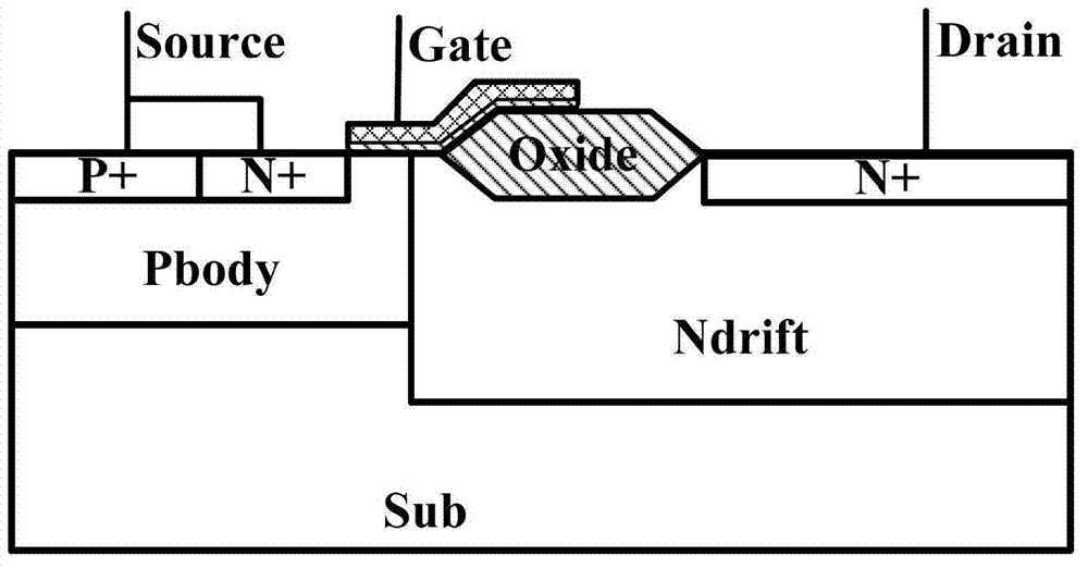
[0004] Unlike low-voltage MOS devices, due to the limitation of withstand voltage, ordinary high-voltage MOS devices will have a drift region Ndrift (such as figure 1 shown), the doping concentration of this drift region is low and the length is relatively long
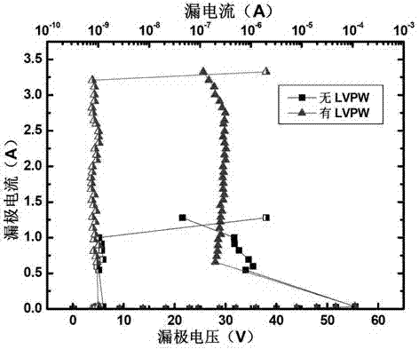
However, since LDMOS is a surface-type device, the Kirk effect usually occurs on the device under ESD stress, and the large electric field and large current are usually concentrated in the bird's beak area at the junction of the thick oxide layer and the active area, and the peak power density is too large, resulting in A lot of heat is easy to burn the device

Method used


Image

  • nLDMOS (Laterally Diffused Metal Oxide Semiconductor) device with ESD (electronic static discharge) protection function
  • nLDMOS (Laterally Diffused Metal Oxide Semiconductor) device with ESD (electronic static discharge) protection function
  • nLDMOS (Laterally Diffused Metal Oxide Semiconductor) device with ESD (electronic static discharge) protection function

Examples


specific Embodiment approach 1

[0021] An nLDMOS device with ESD protection, such as figure 2 As shown, including: N-type or P-type semiconductor substrate Sub, P-type semiconductor base region Pbody located on the surface of N-type or P-type semiconductor substrate Sub, N-type semiconductor drift located on the surface of N-type or P-type semiconductor substrate Sub District Ndrift. The P-type semiconductor base region Pbody and the N-type semiconductor drift region Ndrift are in contact with or separated from each other. The surface of the P-type semiconductor base region Pbody far away from the N-type semiconductor drift region Ndrift has a source P+ contact region and a source N+ contact region, and the source P+ contact region and the source N+ contact region are connected by metal and drawn out as the source of the device. . The surface of the N-type semiconductor drift region Ndrift away from the P-type semiconductor base region Pbody has a drain N+ contact region, and the drain N+ contact region i...

specific Embodiment approach 2

[0022] like image 3 shown in figure 2 On the basis of the shown structure, the surface of the substrate Sub has a deep N-type semiconductor diffusion region DNW, and the P-type semiconductor base region Pbody and the N-type semiconductor drift region Ndrift are made on the surface of the deep N-type semiconductor diffusion region DNW; and the P-type The semiconductor base region Pbody and the N-type semiconductor drift region Ndrift are separated from each other, and the oxide layer Oxide covers the surface of the N-type semiconductor drift region Ndrift close to the P-type semiconductor base region Pbody and part of the surface of the deep N-type semiconductor diffusion region DNW.

specific Embodiment approach 3

[0023] like Figure 4 shown in figure 2 On the basis of the shown structure, the surface of the substrate Sub has an N-type epitaxial layer Nepi, the P-type semiconductor base region Pbody and the N-type semiconductor drift region Ndrift are made on the surface of the N-type epitaxial layer Nepi, and the N-type epitaxial layer Nepi is connected with the substrate There is also an N+ buried layer NBL between the bottom Sub; the P-type semiconductor base region Pbody and the N-type semiconductor drift region Ndrift are separated from each other, and the oxide layer Oxide covers the surface of the N-type semiconductor drift region Ndrift close to the P-type semiconductor base region Pbody and covers Part of the N-type epitaxial layer Nepi surface.

[0024] Figure 5 It is an embodiment of the third structure (specific implementation mode 3) of the present invention in practical application. In the figure, the gate and source of the LDMOS are grounded, and the drain is connecte...


PUM


Abstract

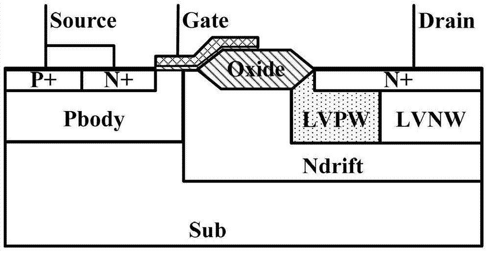
An nLDMOS (Laterally Diffused Metal Oxide Semiconductor) device with an ESD (electronic static discharge) protection function belongs to the field of electronic technique. A P trap and an N trap for manufacturing a low-voltage device are introduced between the drift region and the drain electrode contact region of a conventional nLDMOS device, and the ESD current is enabled to flow through the deeper region of the device, so that the peak power density under ESD stress is reduced, the current is prevented from centralizing in the surface of the device, the uniformity on heat dissipation of the device is improved on the basis of greatly improving the reliability of the beak position of a drain terminal, and the ESD protection capacity of the device is accordingly improved. The nLDMOS device with the ESD protection function is compliable with the techniques of Bipolar CMOS (Complementary Metal-Oxide-Semiconductor Transistor) and DMOS (Double Diffusion Metal-Oxide-Semiconductor), and the cost of the device is not remarkably increased.

Description

technical field [0001] The invention belongs to the field of electronic technology, and relates to the electrostatic discharge (ElectroStatic Discharge, referred to as ESD) protection circuit technology of semiconductor integrated circuit chips, especially an n-channel lateral double-diffusion MOSFET (n-channel Lateral Double-Diffusion MOSFET) for ESD protection. Diffusion MOSFET, referred to as nLDMOS) structure. Background technique [0002] Electrostatic discharge is a common phenomenon in the process of manufacturing, production, assembly, testing and transportation of integrated circuit devices or chips. Electrostatic discharge can cause chip performance degradation or direct damage. According to statistics, ESD damage accounts for as high as 30% of chip damage. Therefore, improving the anti-ESD capability of integrated circuits has very important practical significance. [0003] The essence of ESD failure can be high power or large electric field. The former causes ...

Claims


Application Information

Patent Timeline
IPC IPC(8): H01L29/78H01L29/06
Inventor 张波樊航蒋苓利吴道训何川
Owner UNIV OF ELECTRONIC SCI & TECH OF CHINA
Learn More