Method for reducing metal secondary electron yield by utilizing regular array structure

A technology of secondary electron emission and array structure, which is applied in the direction of microstructure technology, microstructure device, and manufacturing microstructure device, etc. It can solve the problem of deterioration of electromagnetic wave transmission characteristics of microwave devices, increase of microwave loss, and failure of device or system performance indicators to meet requirements etc. to achieve the effect of reducing the secondary electron emission coefficient

Inactive Publication Date: 2012-11-28
XI AN JIAOTONG UNIV +1
View PDF5 Cites 15 Cited by
  • Summary
  • Abstract
  • Description
  • Claims
  • Application Information

AI Technical Summary

Problems solved by technology

Although foreign countries have realized millimeter-scale regular structures to suppress SEY, in certain occasions (for example, high-power microwave systems), this millimeter-scale surface structure can suppress SEY but will lead to deterioration of other aspects of the system. For example, microwave loss will be significantly increased due to this millimeter-scale undulation structure, and the electromagnetic wave transmission characteristics of microwave devices may also be deteriorated due to this structure, resulting in device or system performance indicators that cannot meet the requirements

Method used


Image

  • Method for reducing metal secondary electron yield by utilizing regular array structure
  • Method for reducing metal secondary electron yield by utilizing regular array structure
  • Method for reducing metal secondary electron yield by utilizing regular array structure

Examples


Embodiment Construction

[0034] The present invention will be described in detail below in conjunction with the accompanying drawings.

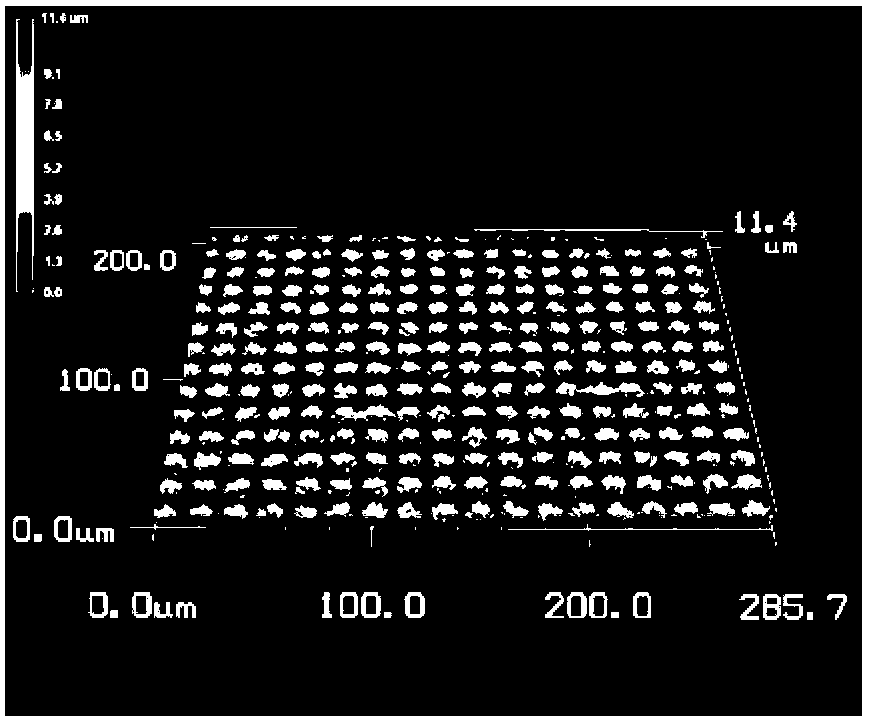
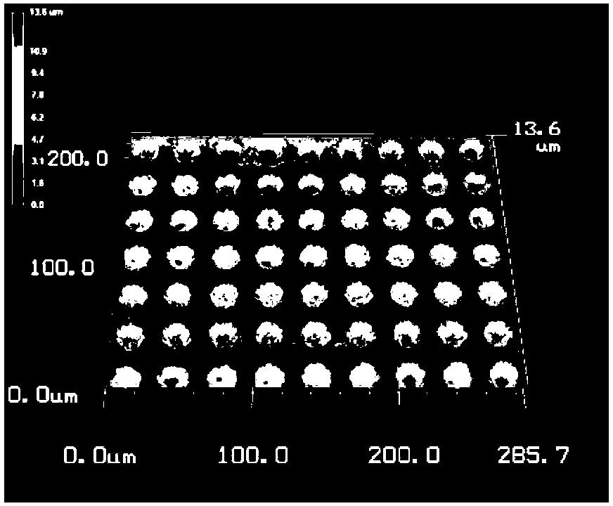
[0035] The process of a typical micron-scale array structure on a metal surface is as follows: figure 1 shown.

[0036] This patent proposes a method for effectively suppressing the secondary electron emission coefficient of the metal surface. This method uses a typical semiconductor photolithography process to prepare micron-scale array structures on the surface of common metals, thereby achieving the purpose of suppressing SEY. The method mainly includes the following processing steps: Ultrasonic cleaning of the metal sample to be treated with absolute ethanol and deionized water to remove surface contamination; spin coating of the sample at a certain rotation speed (according to the required array pattern and mask Plate parameters determine whether to use positive photoresist or negative photoresist); bake the sample after coating at a certain temperature for a ...


PUM


Abstract

The invention provides a method for inhibiting a metal surface SEY (Secondary Electron Yield) by utilizing a regular array structure. The regular array structure is realized by utilizing an image photolithography process of a semiconductor device field. A typical array structure can adopt a circular hole or a rectangular groove structure; and the size of the structure ranges from several microns to dozens of microns. The shape of the regular array structure is determined by a designed mask, and the depth/width ratio of a regular trap is determined by etching time. Under the condition of the same depth/width ratio and porosity, the inhibiting effect of a circular hole trap surface SEY is better than that of a rectangular groove trap surface; with the regard to the same array structure, the porosity is greater when the depth/width ratio is greater, and the SEY inhibiting effect is better. The technology disclosed by the invention has the potential application value on inhibiting a micro-discharging effect of a metal microwave part in a satellite load and a particle accelerator, namely the surface SEY is reduced through a surface imaged photolithography under the precondition of not changing a surface metal material of the part, so that the micro-discharging effect can be inhibited in a greater extent. Meanwhile, the technology is also applicable to various special application fields needing to carry out metal surface SEY inhibition, such as a traveling wave tube collection electrode and the like; and the method has certain universality.

Description

Technical field: [0001] The patent of the invention relates to the field of surface treatment of high-power microwave components, which is used to suppress the secondary electron emission coefficient of the metal surface, so that the application of the new method can greatly improve the working performance of related components and systems. It specifically involves the use of micropattern lithography in the semiconductor field to form a regular array structure on the metal surface. This technology can significantly suppress the secondary electron emission coefficient of the metal surface and provide an effective method for improving the performance of high-power microwave components. Background technique: [0002] Secondary electron emission refers to the phenomenon that when electrons of a certain energy are incident on a solid surface, electrons are emitted from the solid surface. Usually, the incident electrons are called initial electrons, and the outgoing electrons are c...

Claims


Application Information

Patent Timeline
Patent Type & Authority Applications(China)
IPC IPC(8): B81C1/00
Inventor 贺永宁叶鸣崔万照王瑞胡天存黄光孙
Owner XI AN JIAOTONG UNIV
Why Eureka
Try Eureka