Transistor forming method

A transistor and gate structure technology, applied in the manufacture of transistors, semiconductor devices, semiconductor/solid-state devices, etc., can solve the problems of unsatisfactory transistor performance, high junction capacitance and junction current, improve standard and reduce junction leakage current. , the effect of improving device performance

Active Publication Date: 2012-11-28
SEMICON MFG INT (SHANGHAI) CORP
View PDF5 Cites 3 Cited by
  • Summary
  • Abstract
  • Description
  • Claims
  • Application Information

AI Technical Summary

Problems solved by technology

[0008] In practice, it is found that the junction capacitance and junction current between the source / drain region and the substrate of the transistor formed by the existing method are relatively high, and the performance of the transistor is not ideal

Method used


Image

  • Transistor forming method
  • Transistor forming method
  • Transistor forming method

Examples


Embodiment Construction

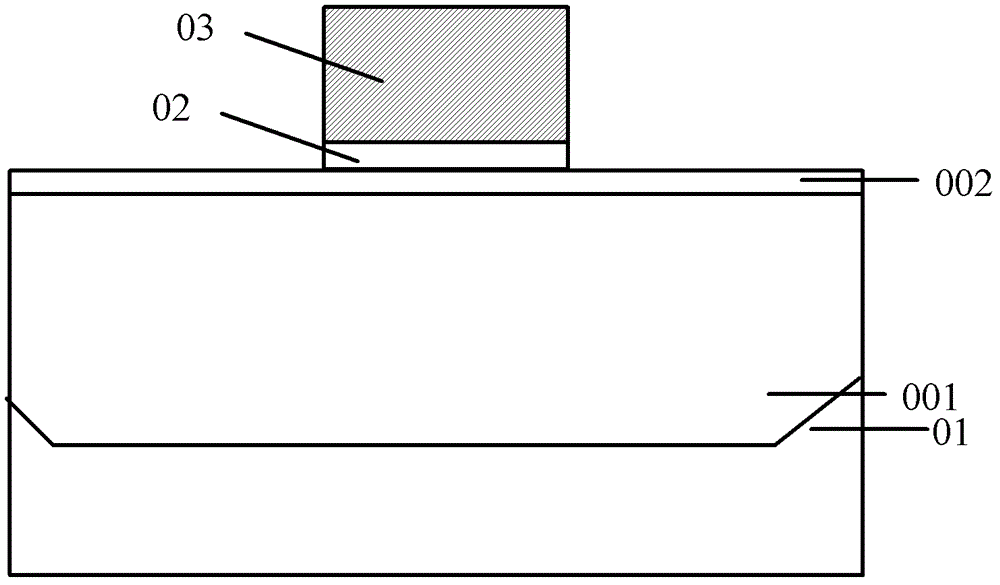
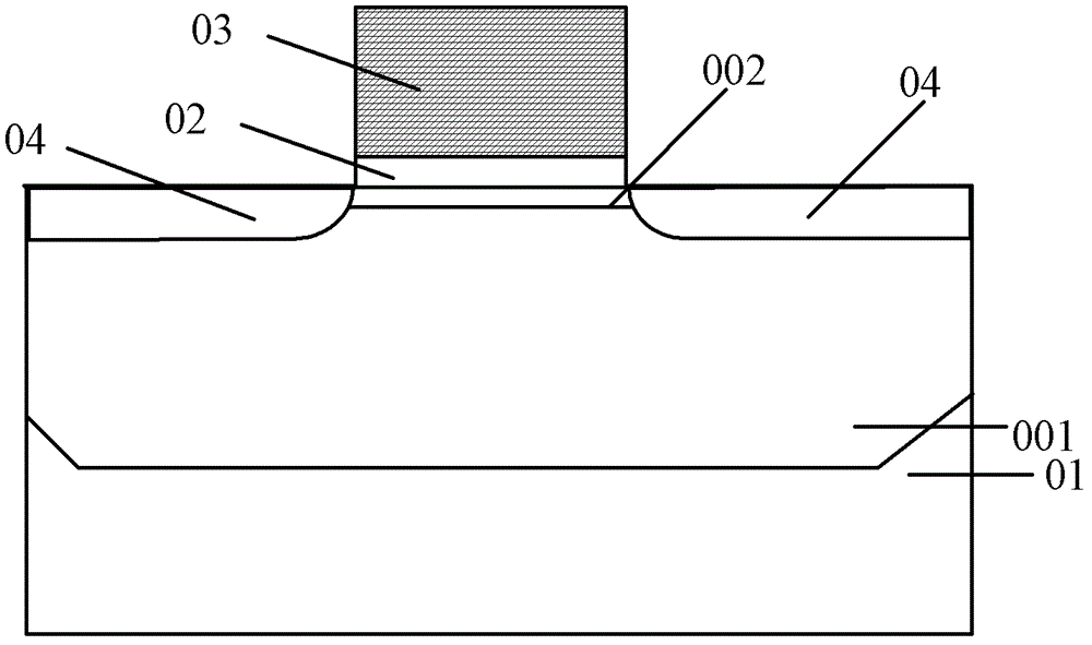
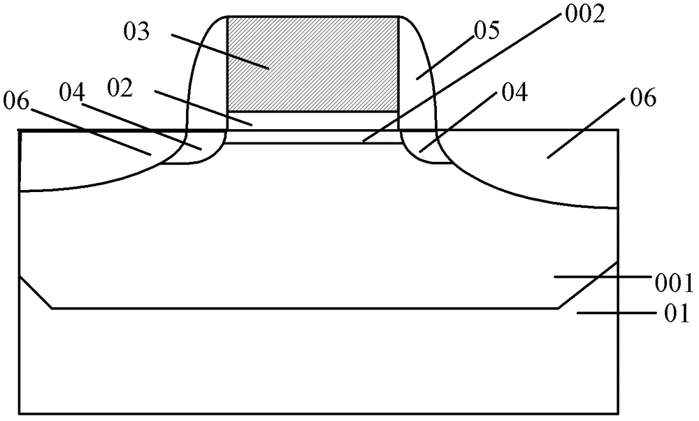
[0032] The inventors found that, in theory, the ions for adjusting the threshold voltage only need to be distributed near the substrate surface below the gate oxide layer, but the threshold voltage ion implantation of the prior art is very important in the process of forming the gate structure and the source and drain regions. However, there is a high-temperature environment or heat treatment process in the formation of the gate structure and the source and drain regions, which will strengthen the diffusion of ions that adjust the threshold voltage, making the ions diffuse into the substrate, increasing the source / drain region and the substrate. The junction capacitance between the bottoms increases the junction leakage current and reduces the operating speed and performance of the device.

[0033] In order to solve the above problems, the inventor provides a method for forming a transistor, including: providing a substrate; forming a well region in the substrate; forming a gat...


PUM


Abstract

The invention provides a transistor forming method. The transistor forming method comprises the following steps of: providing a substrate; forming a well region in the substrate; forming a gate structure on the surface of the substrate, wherein the gate structure comprises a gate oxide layer and a gate positioned on the surface of the gate oxide layer; forming a source region and a drain region which are positioned in the substrate on the two sides of the gate structure; and after forming the source region and the drain region, doping first ions in the substrate to adjust a threshold voltage. The first ions for adjusting the threshold voltage are injected after the formation of the source region and the drain region, so that the influence on the diffusion of the first ions caused by a heat treatment process before injecting the first ions is reduced; most of the first ions are distributed close to the surface of the substrate; the concentration of the first ions diffused in the substrate is reduced; the junction capacitance between the source region / drain region and the substrate is reduced; the junction drain current is reduced; the operation speed of a device is increased; and the performance of the device is improved.

Description

technical field [0001] The invention relates to the field of semiconductors, in particular to a method for forming a transistor. Background technique [0002] Metal-oxide-semiconductor (MOS) transistors are the most basic devices in semiconductor manufacturing. They are widely used in various integrated circuits. According to the main carrier and the type of doping during manufacturing, they are divided into NMOS and PMOS transistors. [0003] The prior art provides a method for forming a transistor. Please refer to Figure 1 to Figure 3 , is a schematic cross-sectional structure diagram of a method for forming a transistor in the prior art. [0004] Please refer to figure 1 , provide a substrate 01, perform ion implantation on the substrate 01, and perform heat treatment on it to form a well region 001; perform ion implantation on the substrate 01 to form an ion region 002, and the ion region 002 is located on the substrate 01 surface, so as to adjust the threshold volt...

Claims


Application Information

Patent Timeline
Patent Type & Authority Applications(China)
IPC IPC(8): H01L21/336H01L21/265
CPCH01L29/66537H01L21/265H01L21/2652H01L29/6659H01L29/66545
Inventor 赵猛
Owner SEMICON MFG INT (SHANGHAI) CORP
Why Eureka
Try Eureka