
Light-emitting diode device and production method thereof
A technology of light-emitting diodes and devices, which is applied in the direction of semiconductor devices, electrical solid devices, electrical components, etc., can solve the problems of deterioration of light-emitting chips, glue solution that cannot withstand high temperatures, and cannot ensure that chips are evenly coated with phosphors, etc.
- Summary
- Abstract
- Description
- Claims
- Application Information
AI Technical Summary
Problems solved by technology
Method used
Image

Examples
Embodiment 1
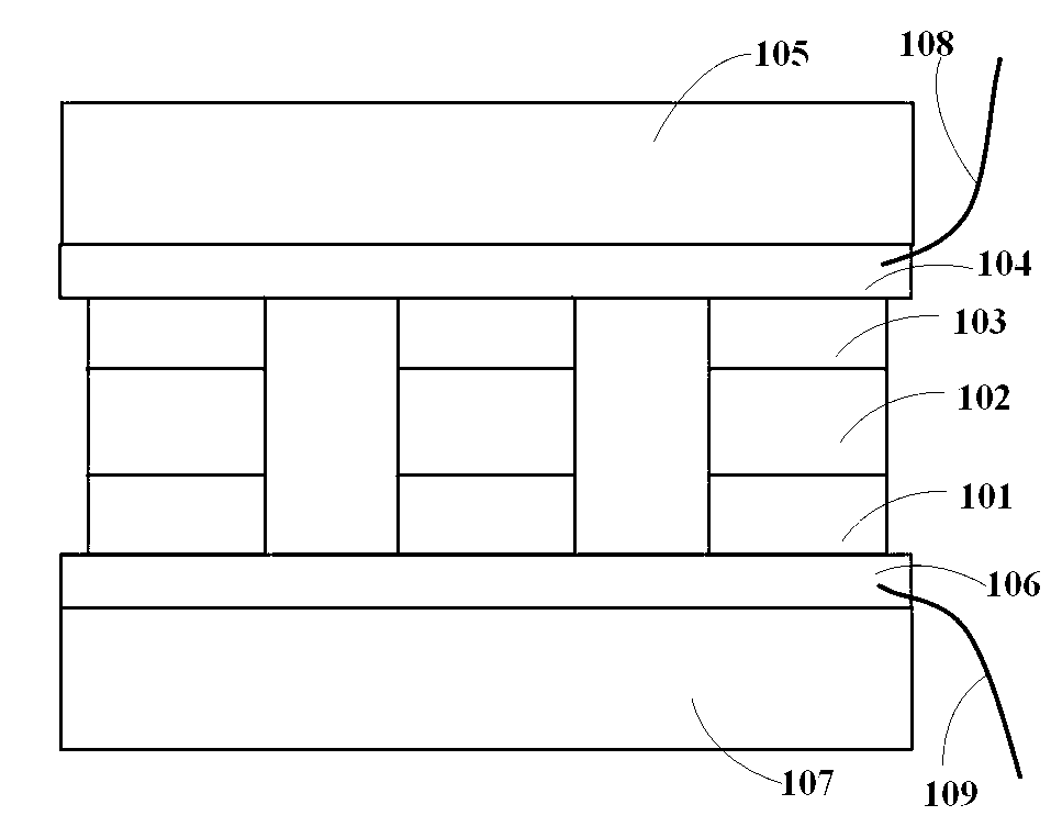
[0041] Such as Figure 10 A light-emitting diode device shown includes: three LED epitaxial layers arranged at intervals, wherein the epitaxial layer includes a first semiconductor layer 101, a light-emitting layer 102 and a second semiconductor layer 103; it is composed of a transparent glass 107 and a transparent conductive layer 106 The first transparent conductive glass structure is formed on the first semiconductor layer 101 and is used to connect the negative electrode 109 of the power supply; the second transparent conductive glass structure composed of transparent glass 105 and transparent conductive layer 104 is formed on the second On the semiconductor layer 103 , it is used to connect the positive electrode 108 of the power supply.
[0042] Specifically, the above light-emitting diode device includes: 3 LED epitaxial layers arranged at intervals, wherein the epitaxial layer includes an N-GaN layer 101, a light-emitting layer 102 and a P-GaN layer 103; a transparent ...
Embodiment 2
[0054] Such as Figure 17 A light-emitting diode device shown includes: three LED epitaxial layers arranged at intervals, wherein the epitaxial layer includes a first semiconductor layer 201, a light-emitting layer 202 and a second semiconductor layer 203; a reflective layer 206 and a heat dissipation substrate 207 The first substrate structure is formed on the first semiconductor layer 201 and is used to connect the negative electrode 210 of the power supply; the second substrate structure containing phosphor powder composed of transparent glass 205 and transparent conductive layer 204 is formed on the second semiconductor layer Layer 203 is used to connect the positive electrode 209 of the power supply.
[0055] Specifically, the above light-emitting diode device includes: 3 LED epitaxial layers arranged at intervals, wherein the epitaxial layer includes an N-GaN layer 201, a light-emitting layer 202 and a P-GaN layer 203; 207, the first reflective and heat-dissipating subs...
Embodiment 3
[0066] Such as Figure 18 As shown, the light-emitting diode device is different from Example 1 in that the number of LED epitaxial layers is 5, which can form a high-density arrangement; the first substrate structure is composed of a transparent conductive substrate structure containing phosphor, wherein the transparent conductive substrate structure It is composed of transparent flexible plastic 307 and transparent ITO conductive layer 306 .
[0067] The manufacturing method of the above-mentioned light-emitting diode device differs from Embodiment 2 in that:
[0068] In order to improve the light conversion efficiency more effectively, the first substrate is a transparent conductive substrate structure containing phosphor powder, which can form a sandwich structure with the LED epitaxial layer and the second substrate structure containing phosphor powder, forming an all-round non-blocking positive and negative metal electrodes The white light-emitting diode can more ...
PUM
 Abstract
Description
Claims
Application Information