
Formation method of deep groove super positive-negative (PN) junction

A technology of deep trenches and PN junctions, applied in electrical components, semiconductor/solid-state device manufacturing, circuits, etc., can solve problems such as high cost and difficult process control, achieve low cost, avoid Si device parameter instability, and improve efficiency high effect

Active Publication Date: 2012-12-12
CSMC TECH FAB2 CO LTD
View PDF3 Cites 0 Cited by
  • Summary
  • Abstract
  • Description
  • Claims
  • Application Information

AI Technical Summary

Problems solved by technology

[0008] However, in the technology using CMP, because the CMP equipment of the general production line is used in the back channel, it cannot be mixed with the equipment for processing the super PN junction. Therefore, the method of manufacturing the super PN junction using CMP planarization must use special CMP equipment As a result, the process control is difficult and the cost is high

Method used


Image

  • Formation method of deep groove super positive-negative (PN) junction
  • Formation method of deep groove super positive-negative (PN) junction
  • Formation method of deep groove super positive-negative (PN) junction

Examples


Embodiment Construction

[0032] Presented below are some of the many possible embodiments of the invention, intended to provide a basic understanding of the invention. It is not intended to identify key or critical elements of the invention or to delineate the scope of protection.

[0033] In order to make the object, technical solution and advantages of the present invention clearer, the present invention will be further described in detail below in conjunction with the accompanying drawings.

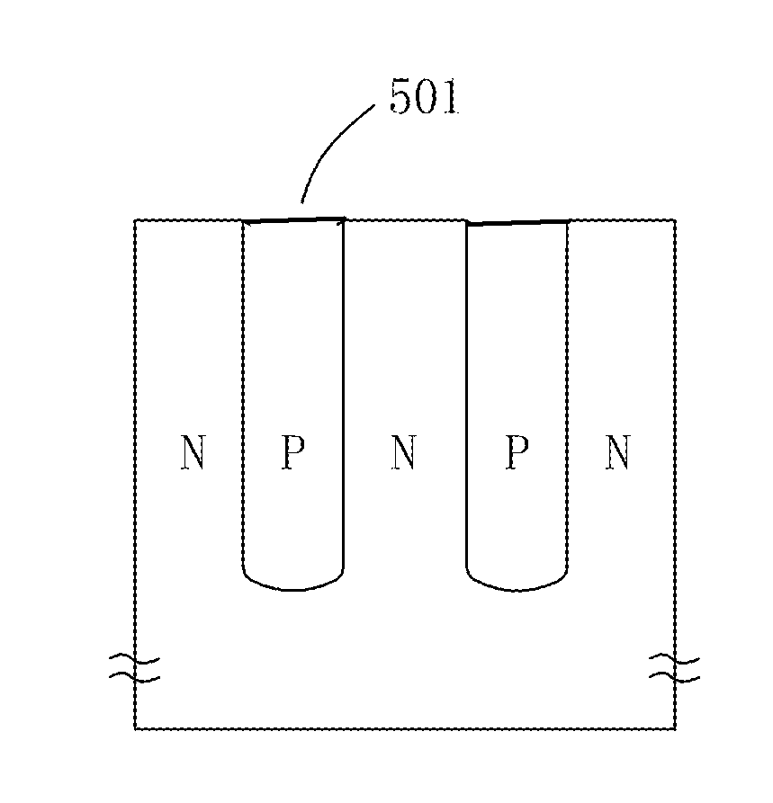
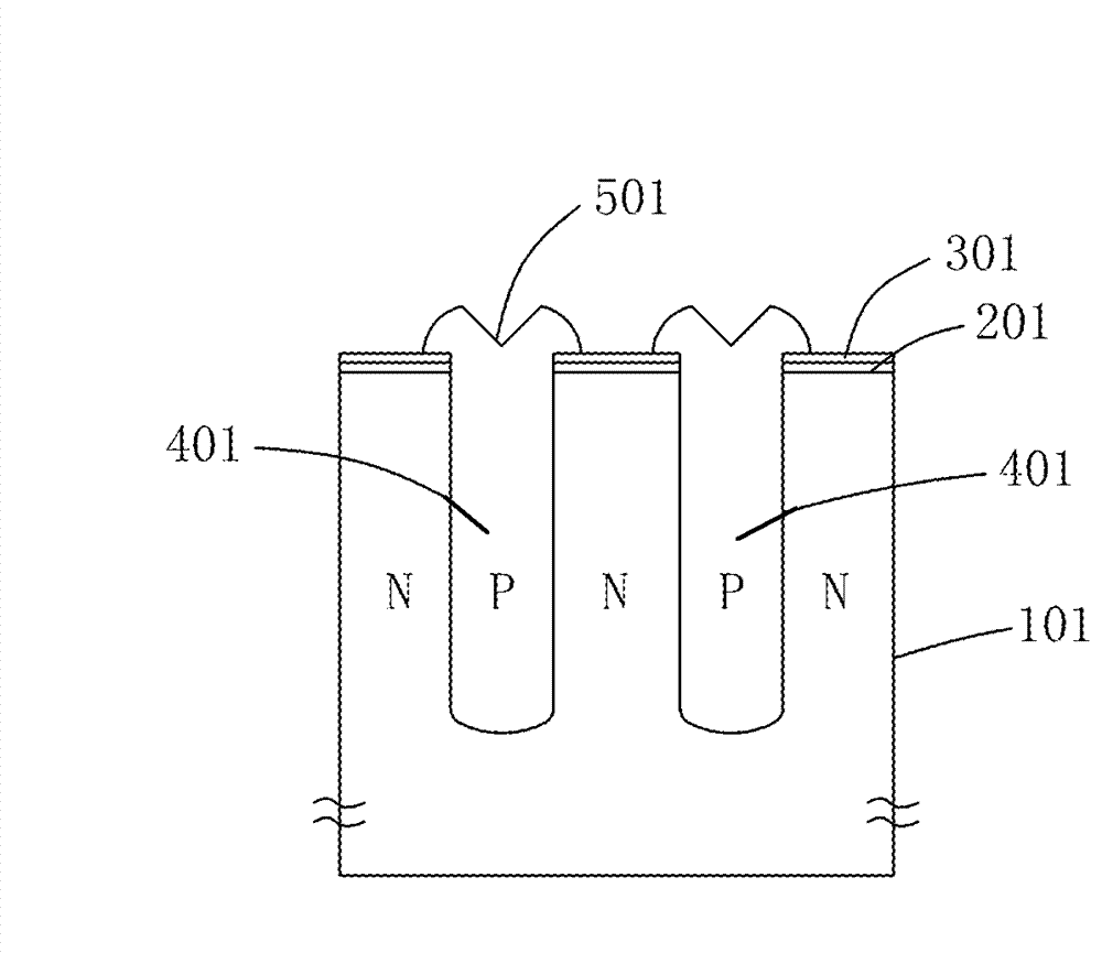
[0034] Below, refer to Figure 1 ~ Figure 4 , a method for forming a deep trench super PN junction according to an embodiment of the present invention will be described.

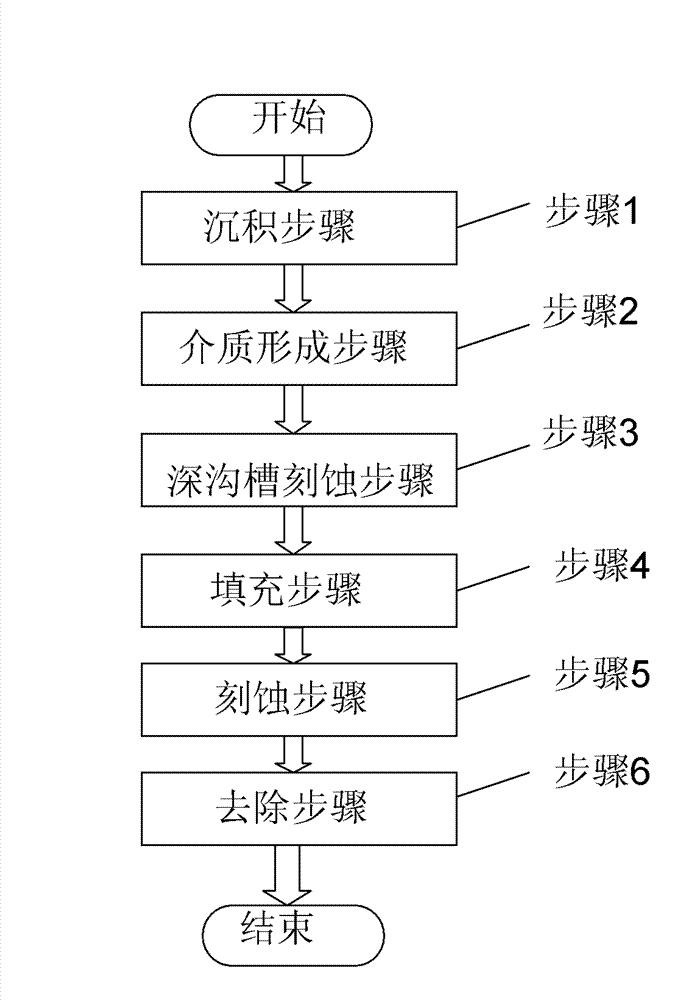
[0035] figure 1 It is an overall flowchart showing the process of forming a super PN junction according to an embodiment of the present invention.

[0036] First, if figure 1 Shown, super PN junction forming method of the present invention mainly comprises:

[0037] Step 1: A deposition step of depositing an epitaxial layer on a substra...


PUM


Abstract

The invention relates to a formation method of a deep groove super PN junction. The method comprises the steps of depositing an epitaxial layer on a substrate; forming a first dielectric layer and a second dielectric layer on the epitaxial layer sequentially; forming a deep groove on the epitaxial layer; filling the deep groove with epitaxial materials till the specified height of the second dielectric layer is exceeded; etching epitaxial materials, the first dielectric layer and the second dielectric layer till the interface positions of the first dielectric layer and epitaxial materials with etching gases; and removing the first dielectric layer and the second dielectric layer to achieve planarization of epitaxial materials. By the aid of the formation method, planarization of silicon can be achieved by using the method which is compatible with existing processes, the formation method has the advantages of being simple in process, high in efficiency and low in process cost, and the problem that parameters of silicon (Si) devices are not stable due to chemical-mechanical polishing (CMP) can be effectively solved.

Description

technical field [0001] The present invention relates to semiconductor manufacturing technology, in particular to a deep trench super PN junction (Super Junction) manufacturing technology. Background technique [0002] In the field of semiconductors, the super PN junction (Super Junction) technology used to improve the performance of power MOS plays a very significant role in the high voltage field. [0003] The traditional manufacturing process of super PN junction mainly adopts the methods of deep trench etching, epitaxial filling, and silicon CMP planarization. Specifically, the method for forming a super PN junction in the traditional technology includes the following steps: [0004] Step 1: Deposit a single thick epitaxial layer (N-type) on the N+ substrate silicon wafer; [0005] Step 2: Form a deep trench in the epitaxial layer, specifically, first grow a thermal oxide layer, then deposit a silicon nitride layer, and then deposit a plasma-enhanced oxide layer, etch t...

Claims


Application Information

Patent Timeline
Patent Type & Authority Applications(China)
IPC IPC(8): H01L21/18H01L21/306
CPCH01L21/3105H01L29/0634H01L21/3065
Inventor 吴宗宪王根毅袁雷兵吴芃芃
Owner CSMC TECH FAB2 CO LTD
Learn More