

Process of growing self-organized Ge quantum dot by means of ion beam sputtering in low growth beam flux
A technology of ion beam sputtering and quantum dots, which is applied in the field of preparation of nano-quantum materials, can solve the problems of unfavorable large-scale production, low production efficiency, and high production cost, and achieve the effects of low price, improved production efficiency, and uniform size
- Summary
- Abstract
- Description
- Claims
- Application Information
AI Technical Summary
Problems solved by technology
Method used
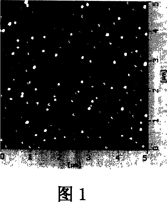
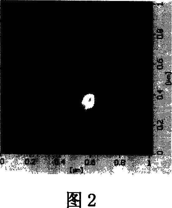
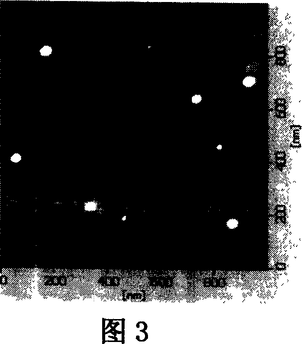
Image

Examples
Embodiment 1
[0021] The equipment used is the ion beam sputtering chamber of the FJL560III type ultra-high vacuum multi-target magnetron and ion beam combined sputtering equipment, and a Kaufman ion gun is placed in the growth chamber. The materials used are: the target material is a high-purity Ge square target of 5N (above 99.999%), a high-purity Si square target of 5N (above 99.999%), and the sputtering gas is a high-purity argon gas of 5N (above 99.999%). A P-type single crystal Si sheet with a crystal orientation of (100) is used as a substrate, and the resistivity is 5Ω / cm. For ultrasonic cleaning, a commercially available ultrasonic cleaner was used.
[0022] specifically is:
[0023] 1. Processing of silicon (Si) base material:
[0024] A, select the Si substrate material whose crystal orientation is (100), and ultrasonically clean it with acetone and absolute ethanol for 20 minutes respectively to remove surface organic and inorganic impurities;
[0025] B. Put the cleaned Si s...
Embodiment 2
[0031] The equipment and materials used are all the same as in Example 1. specifically is:
[0032] 1. Processing of silicon (Si) base material:
[0033] A, select the Si substrate material whose crystal orientation is (100), and ultrasonically clean it with acetone and absolute ethanol for 20 minutes respectively to remove surface organic and inorganic impurities;
[0034] B. Put the cleaned Si sheet into the following solution and soak for 20s to rinse off the oxide layer: the concentration is 40% HF: H 2 O=1:20.
[0035] 2. Alternate sputtering of Ge / Si multilayer self-organized Ge quantum dots by ion beam:
[0036] A. Place the pre-treated Si substrate material in the sputtering chamber until the background vacuum in the sputtering chamber is greater than 4.0×10 -4 Pa, adjust the temperature of the sputtering chamber to 400°C, fill the sputtering chamber with Ar gas with a purity of 5N until the pressure of the sputtering chamber is 4.0×10 -2 Pa;
[0037]B. Under the...
Embodiment 3
[0040] The equipment and materials used are all the same as in Example 1. specifically is:
[0041] 1. Processing of silicon (Si) base material:
[0042] A, select the Si substrate material whose crystal orientation is (100), and ultrasonically clean it with acetone and absolute ethanol for 20 minutes respectively to remove surface organic and inorganic impurities;
[0043] B. Put the cleaned Si sheet into the following solution and soak for 20s to rinse off the oxide layer: the concentration is 40% HF: H 2 O=1:20.
[0044] 2. Alternate sputtering of Ge / Si multilayer self-organized Ge quantum dots by ion beam:
[0045] A. Place the pre-treated Si substrate material in the sputtering chamber until the background vacuum in the sputtering chamber is greater than 4.0×10 -4 Pa, adjust the temperature of the sputtering chamber to 100°C, fill the sputtering chamber with Ar gas with a purity of 5N until the pressure of the sputtering chamber is 2.0×10 -2 Pa;
[0046] B. Under th...
PUM
| Property | Measurement | Unit |
|---|---|---|
| thickness | aaaaa | aaaaa |
| thickness | aaaaa | aaaaa |
| thickness | aaaaa | aaaaa |
Abstract
Description
Claims
Application Information