Manufacturing method of array substrate, array substrate and display device
A manufacturing method and array substrate technology, which are applied in semiconductor/solid-state device manufacturing, optics, instruments, etc., can solve the problem of excessive third via etching, incomplete array substrate etching, affecting the yield and performance of the array substrate, etc. problems, to achieve the effect of improving yield and performance
- Summary
- Abstract
- Description
- Claims
- Application Information
AI Technical Summary
Problems solved by technology
Method used
Image

Examples
Embodiment Construction
[0045] The following will clearly and completely describe the technical solutions in the embodiments of the present invention with reference to the accompanying drawings in the embodiments of the present invention. Obviously, the described embodiments are only some, not all, embodiments of the present invention.
[0046] In order to make the advantages of the technical solution of the present invention clearer, the present invention will be described in detail below in conjunction with the accompanying drawings and embodiments.
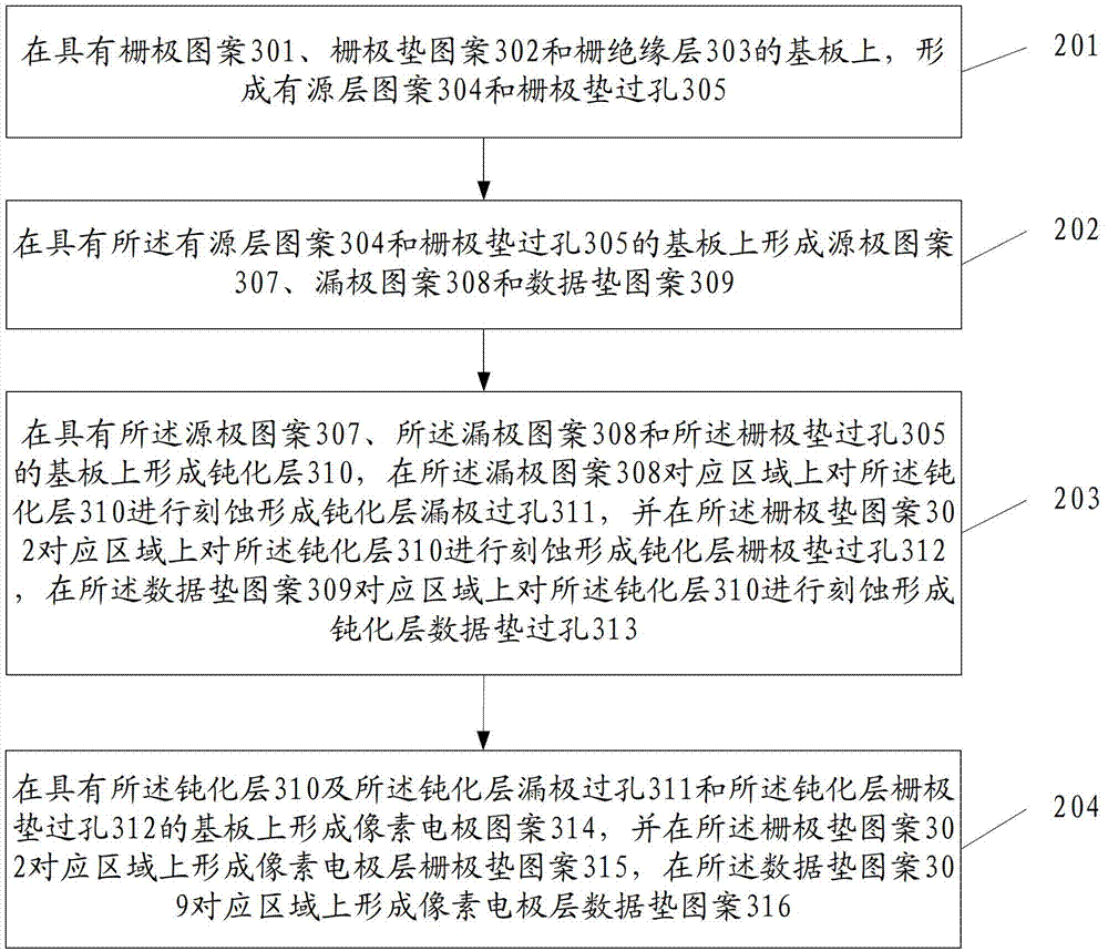
[0047] Such as figure 2 and image 3 As shown, the manufacturing method of the array substrate provided by the embodiment of the present invention includes:
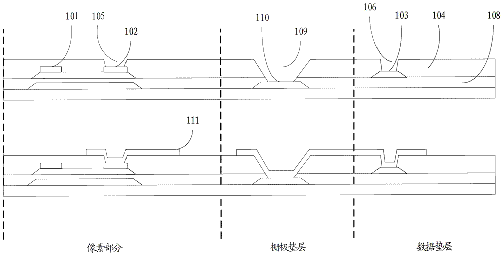
[0048] Step 201, on the substrate having gate pattern 301, gate pad Gate Pad pattern 302 and gate insulating layer 303, form active layer pattern 304 and gate pad via hole 305; A gate line pattern is formed simultaneously with the pad pattern 302 (the gate line pattern is not shown).
[0049]...
PUM
| Property | Measurement | Unit |
|---|---|---|
| thickness | aaaaa | aaaaa |
Abstract
Description
Claims
Application Information
 - R&D
- Intellectual Property
- Life Sciences
- Materials
- Tech Scout
- Unparalleled Data Quality
- Higher Quality Content
- 60% Fewer Hallucinations
Browse by: Latest US Patents, China's latest patents, Technical Efficacy Thesaurus, Application Domain, Technology Topic, Popular Technical Reports.
© 2025 PatSnap. All rights reserved.Legal|Privacy policy|Modern Slavery Act Transparency Statement|Sitemap|About US| Contact US: help@patsnap.com