A preparation method of a chip type ceramic sensitive element and corresponding products thereof

A technology of sensitive components and ceramics, which is applied in the field of sensing and measurement, can solve the problems of silver ion non-ohmic contact, silver-tin solder layer blending, adverse effects on the quality of final products, unfavorable standardized production, etc., to achieve a high degree of automation and eliminate non-ohmic The effect of contact phenomenon and avoiding wire bending or even breaking

Inactive Publication Date: 2015-08-26
HUAZHONG UNIV OF SCI & TECH
View PDF7 Cites 0 Cited by
  • Summary
  • Abstract
  • Description
  • Claims
  • Application Information

AI Technical Summary

Problems solved by technology

Although the silver electrode has the advantage of good conductivity, there are problems of high material cost, especially the easy migration of silver ions to produce defects such as non-ohmic contact and silver-tin solder layer fusion; secondly, when performing glass packaging or single-ended lead epoxy When packaged in the same way, the lead wires of the electrodes of the ceramic sensitive element need to be bent, and sometimes even broken, which will adversely affect the quality of the final product; in addition, in the preparation method of the prior art, the sensitive element is executed after the finished product is packaged. Resistance test, so that even if the resistance test is unqualified, it cannot be adjusted, which correspondingly causes problems such as low yield, increased cost, and unfavorable standardized production.

Method used


Image

  • A preparation method of a chip type ceramic sensitive element and corresponding products thereof
  • A preparation method of a chip type ceramic sensitive element and corresponding products thereof
  • A preparation method of a chip type ceramic sensitive element and corresponding products thereof

Examples


Embodiment Construction

[0039]In order to make the object, technical solution and advantages of the present invention clearer, the present invention will be further described in detail below in conjunction with the accompanying drawings and embodiments. It should be understood that the specific embodiments described here are only used to explain the present invention, not to limit the present invention.

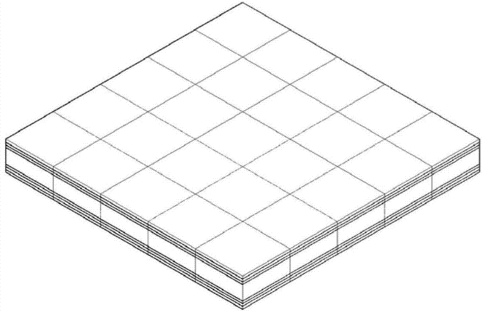
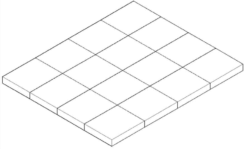
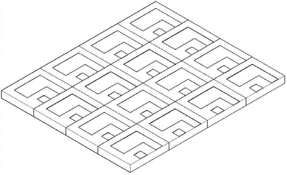
[0040] Figure 1~8 A schematic diagram of the different structures obtained during the preparation method according to the invention is shown. like figure 1 As shown in , first, the preparation steps of the sensitive element body are performed. Taking NTC ceramics as an example, the upper and lower surfaces of NTC ceramics cut into larger pieces (for example, φ50mm disc shape or 50mm×50mm rectangle) can be printed, evaporated, sputtered, etc. respectively. A metal conductive layer is attached to the NTC ceramic sheet. In this embodiment, the metal conductive layer used is a copper layer, and the...


PUM

PropertyMeasurementUnit
thicknessaaaaaaaaaa

Abstract

The invention discloses a preparation method for a chip-type ceramic sensitive element and a corresponding product thereof. The method comprises the steps of respectively processing a metal conducting layer, a transition layer and an easily-welding layer in sequence on the upper surface and the lower surface of a ceramic chip to form an upper electrode and a lower electrode, cutting the ceramic chip into a plurality of sensitive element main bodies, processing a plurality of rectangle areas used for placing the single sensitive element main body on a substrate, respectively arranging a first electrode and a second electrode in each rectangle area, leading out the two electrodes in parallel in a way of facing the same side of the rectangle areas which the two electrodes belong to, arranging each sensitive element main body on the first electrode and connecting the upper electrode of each sensitive element main body with the second electrode, sealing and wrapping each sensitive element main body and a connecting guide line of each sensitive element main body, leading out the first electrode and the second electrode through a lead out guide line, and obtaining the finished sensitive element. The preparation method can eliminate non-ohm contact when a silver electrode is adopted, leads out the lead out guide line in parallel without a requirement of being bent, and can obtain products which are good in electricity-conducting property, low in cost and convenient to produce in a standardized mode.

Description

technical field [0001] The invention belongs to the technical field of sensing and measurement, and more specifically relates to a preparation method of a chip type ceramic sensitive element and corresponding products thereof. Background technique [0002] Sensitive components refer to components that can sensitively sense and respond to the measured variable in the system, usually as the part of the sensor that can directly sense the measured variable. Sensitive elements can be divided into mechanical sensitive elements, electromagnetic sensitive elements, optical sensitive elements, electrochemical sensitive elements and microbial sensitive elements according to their detection principles; according to the types of their constituent materials, they can be divided into semiconductor sensitive elements, Metal sensitive components, ceramic sensitive components, organic polymer sensitive components, enzyme sensitive components and microbial sensitive components, etc. In recen...

Claims


Application Information

Patent Timeline
Patent Type & Authority Patents(China)
IPC IPC(8): H01C7/02H01C7/04
Inventor 郝永德漆志明
Owner HUAZHONG UNIV OF SCI & TECH
Why Eureka
Try Eureka