Terminal extension structure and manufacturing method thereof

A technology of junction terminal extension and extension area, which is applied to the junction terminal extension structure of high-voltage IGBT and its manufacturing field, can solve the problems affecting the breakdown voltage and reliability of the device, and the influence of the surface electric field, so as to improve the distribution of the surface electric field and reduce the Area, the effect of reducing the manufacturing cost

Active Publication Date: 2015-07-22
INST OF MICROELECTRONICS CHINESE ACAD OF SCI
View PDF2 Cites 0 Cited by
  • Summary
  • Abstract
  • Description
  • Claims
  • Application Information

AI Technical Summary

Problems solved by technology

[0006] However, the problem with the above-mentioned junction terminal extension structure is that the terminal structure is easily affected by surface charges, such as interface instability and oxide layer interface charges, so that the surface electric field is affected, which in turn affects the breakdown voltage of the device. and reliability

Method used


Image

  • Terminal extension structure and manufacturing method thereof
  • Terminal extension structure and manufacturing method thereof
  • Terminal extension structure and manufacturing method thereof

Examples


Embodiment 1

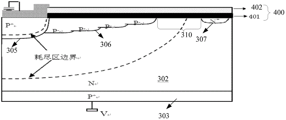
[0047] In this example, refer to image 3 As shown, the junction terminal extension structure includes:

[0048] P + collector area 303;

[0049] P + N on collector region 303 - Drift zone 302;

[0050] N - P on drift zone 302 + The main junction region 305, and the P on the side of the main junction region 305 - Extension 306;

[0051] N outside the extension + cut-off ring 307;

[0052] A stacked structure 400 covering at least the area outside the main junction region 305, the stacked structure 400 includes a semi-insulating polysilicon field plate (SIPOS) 401 and an oxide layer 402, and the oxide layer 402 can be located on the half On the insulating polysilicon field plate 401, there may also be a semi-insulating polysilicon field plate located on the oxide layer, and the semi-insulating polysilicon field plate is located at least part of the extension region 306 and the region between the extension region 306 and the stop ring 307 310 is a continuous structure...

Embodiment 2

[0065] In this example, if Figure 4 As shown, the junction terminal extension structure includes:

[0066] P + collector area 303;

[0067] P + N on collector region 303 - Drift zone 302;

[0068] N - P on drift zone 302 + The main junction region 305, and the P on the side of the main junction region 305 - Extension 306;

[0069] N outside the extension + cut-off ring 307;

[0070] Covering at least the stacked structure 400 outside the main junction region, the field plate is a metal field plate, the stacked structure 400 includes an oxide layer 501 and a metal field plate 502 on the oxide layer 501, the metal The field plate 502 is located on the oxide layer 501 and is a continuous structure located on at least part of the extension region 306 and at least a part of the region between the extension region 306 and the stop ring 307 .

[0071] In this embodiment, the metal field plate can completely cover the extension region and the area between the extension reg...

Embodiment 3

[0081] In this embodiment, by forming a multilevel field plate combined with a polysilicon (POLY) field plate and a metal field plate, the polysilicon (POLY) field plate and the metal field plate are separated by an oxide, while shielding the interface charges, by Optimize the influence of the thickness of the oxide layer on breakdown, improve the phenomenon of surface electric field concentration, suppress premature breakdown, better stabilize the breakdown voltage of the device and improve the reliability of the device.

[0082] refer to Figure 5 As shown, the junction terminal extension structure includes:

[0083] P + collector area 303;

[0084] P + N drift region 302 on collector region 303;

[0085] P on N drift region 302 + The main junction region 305, and the P on the side of the main junction region 305 - Extension 306;

[0086] N outside the extension + cut-off ring 307;

[0087] The stacked structure 400 at least partially covering the area outside the mai...


PUM


Abstract

The invention discloses a terminal extension structure. The terminal extension structure comprises a first conductive type collector region, a second conductive type drift region on the collector region, a first conductive type main junction area on the drift region, a first conductive type extension region on one side of the main junction region, a second conductive type check ring outside the extension region, and a laminated structure at least partially covering a region outside the main junction area, wherein the laminated structure comprises an oxide layer and a field plate; the field plate is of a continuous structure positioned in at least a part of the extension region and on at least a part of a region between the extension region and the check ring; and the field plate is used for screening interface charges to improve the surface electric field distribution. The influence of the interface charges in the extension region and on the outer side of the extension region is screened through the field plate to improve a surface electric field, so as to guarantee the breakdown voltage of a device and improve the reliability of the device; and the terminal extension structure can be applied to a protection terminal of a high-voltage (4500 V or above) IGBT (Insulated Gate Bipolar Translator) device.

Description

technical field [0001] The invention relates to semiconductor manufacturing technology, more specifically, to a junction terminal extension structure of a high-voltage IGBT and a manufacturing method thereof. Background technique [0002] Insulated Gate Bipolar Transistor (IGBT, Insulated Gate Bipolar Transistor) is a new type of high-power device, which combines MOSFET gate voltage control characteristics and low on-resistance characteristics of bipolar transistors, improving device withstand voltage and on-resistance The situation of mutual containment has the advantages of high voltage, high current, high frequency, high power integration density, large input impedance, small on-resistance, and low switching loss. It has gained wide application space in many fields such as frequency conversion home appliances, industrial control, electric and hybrid vehicles, new energy, and smart grid. [0003] An important prerequisite for ensuring the high voltage of the IGBT is an ex...

Claims


Application Information

Patent Timeline
Patent Type & Authority Patents(China)
IPC IPC(8): H01L29/739H01L29/40H01L21/331
CPCH01L29/7395H01L29/402H01L29/0615H01L29/405
Inventor 田晓丽朱阳军吴振兴卢烁今
Owner INST OF MICROELECTRONICS CHINESE ACAD OF SCI
Why Eureka
Try Eureka