Epitaxial growth method for gallium-nitride-based (GaN-based) light-emitting diode (LED)

A technology of light-emitting diodes and epitaxial growth, applied in chemical instruments and methods, crystal growth, single crystal growth, etc., can solve the problems of LED device luminous efficiency and working life attenuation, and the crystal quality of P-type gallium nitride layer is not good enough, etc. Achieve the effects of improving luminous efficiency and working life, convenient operation, and reducing yellow belt

Inactive Publication Date: 2012-12-26
合肥彩虹蓝光科技有限公司
View PDF5 Cites 14 Cited by
  • Summary
  • Abstract
  • Description
  • Claims
  • Application Information

AI Technical Summary

Problems solved by technology

[0004] Aiming at the problem that the crystal quality of the P-type gallium nitride layer in the GaN-based light-emitting diode produced in the prior art is not good enough, which l

Method used


Image

  • Epitaxial growth method for gallium-nitride-based (GaN-based) light-emitting diode (LED)

Examples


Embodiment Construction

[0024] The present invention will be described in detail below in conjunction with specific embodiments. The following examples will help those skilled in the art to further understand the present invention, but do not limit the present invention in any form. It should be noted that those skilled in the art can make several modifications and improvements without departing from the concept of the present invention. These all belong to the protection scope of the present invention.

[0025] Embodiments of the invention were implemented using a Vecco MOCVD system.

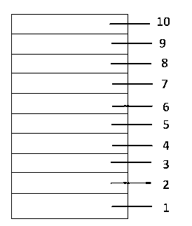
[0026] like figure 1 The shown LED epitaxial structure includes, from bottom to top, substrate 1, low-temperature GaN buffer layer 2, high-temperature GaN buffer layer 3, N-type GaN layer 4, shallow quantum well 5, light-emitting layer multi-quantum well 6, P Type GaN layer 7, P-type AlGaN layer 8, P-type GaN layer 9, and P-type contact layer 10. Its preparation method is as follows:

[0027] A gallium nitride-ba...


PUM


Abstract

The invention relates to an epitaxial growth method for a gallium-nitride-based (GaN-based) light-emitting diode (LED), comprising the following steps of: annealing a substrate, then nitriding; cooling to grow a low temperature GaN buffer layer; rising the temperature of the substrate, thermally annealing the low temperature GaN baffer layer, epitaxially growing the high temperature GaN buffer layer; then growing a layer of an N-type GaN layer with stable doping concentration; growing light quantum well; growing multiple quantum wells of luminescent layer; seventhly, growling a P-type GaN layer with nitrogen (N2) as carrier gas; growing a P-type aluminum gallium nitride (AlGaN) layer; growing the P-type GaN layer; growing a P contact layer; reducing the temperature of a reaction chamber, annealing, then reducing to the room temperature. The method provided by the invention comprises high pressure growth of the P-type GaN layer after the P-type AlGaN layer, a high pressure growth condition can decrease the carbon generated in the epitaxial deposition process, decrease yellow belt and be capable of obtaining high-quality crystal, thereby obtaining a high-quality LED device and improving luminous efficiency and a working life of the device.

Description

[0001] technical field [0002] The invention belongs to the technical field of preparation of gallium nitride-based materials, and in particular relates to a gallium nitride-based light-emitting diode epitaxial growth method. Background technique [0003] The quality of P-type GaN crystal affects the working life and luminous efficiency of the device. The quality of P-type GaN material crystal is not high, which affects the quality and life of the light-emitting device, and will have a serious impact on the light-emitting diode. Only better crystal quality can be obtained. High-quality and long-life gallium nitride-based light-emitting diodes can only be obtained if P-type gallium nitride-based materials are used. Generally, when growing P-type GaN, it is difficult to obtain a P-type GaN layer with high crystal quality. Contents of the invention [0004] Aiming at the problem that the crystal quality of the P-type gallium nitride layer in the GaN-based light-emitting dio...

Claims


Application Information

Patent Timeline
IPC IPC(8): H01L33/00C30B25/02C30B29/38
Inventor 郭丽彬
Owner 合肥彩虹蓝光科技有限公司
Why Eureka
Try Eureka