
Patsnap Eureka
For R&D, Patsnap Eureka makes reading and utilizing patents & technical documents easy.
Patsnap Eureka AIR
Designed for self-driven R&D workflows. Generate viable solutions, solve complex R&D challenges, empower your innovation with AI.

Patsnap Eureka Materials
Designed for material experts only. Revolutionize your material R&D, from search, analyze, to developing new materials.

TechResearch
Generate reliable direction feasibility study reports for your R&D in just a few steps.

TechSeek
Discover and master advanced knowledge NOW. Basics, ideas, possibilities, all at once.

TechMind
As an expert in R&D Theories, TechMind can generates customized viable solutions instantly.

TechRisk
Analyze your overall solution with one click, know your potential R&D risks in advance.

TechMonitor
Get weekly tech updates, stay abreast of the latest tech innovations and key insights.
Method for forming multi-gate device
A device and gate dielectric layer technology, applied in the field of multi-gate device formation, can solve the problems of poor local flatness of the dielectric layer 22, affecting the consistency of parameters between multi-gate devices, and poor uniformity of the dielectric layer 22
- Summary
- Abstract
- Description
- Claims
- Application Information
AI Technical Summary
Problems solved by technology
Method used
Image

Examples
Embodiment Construction
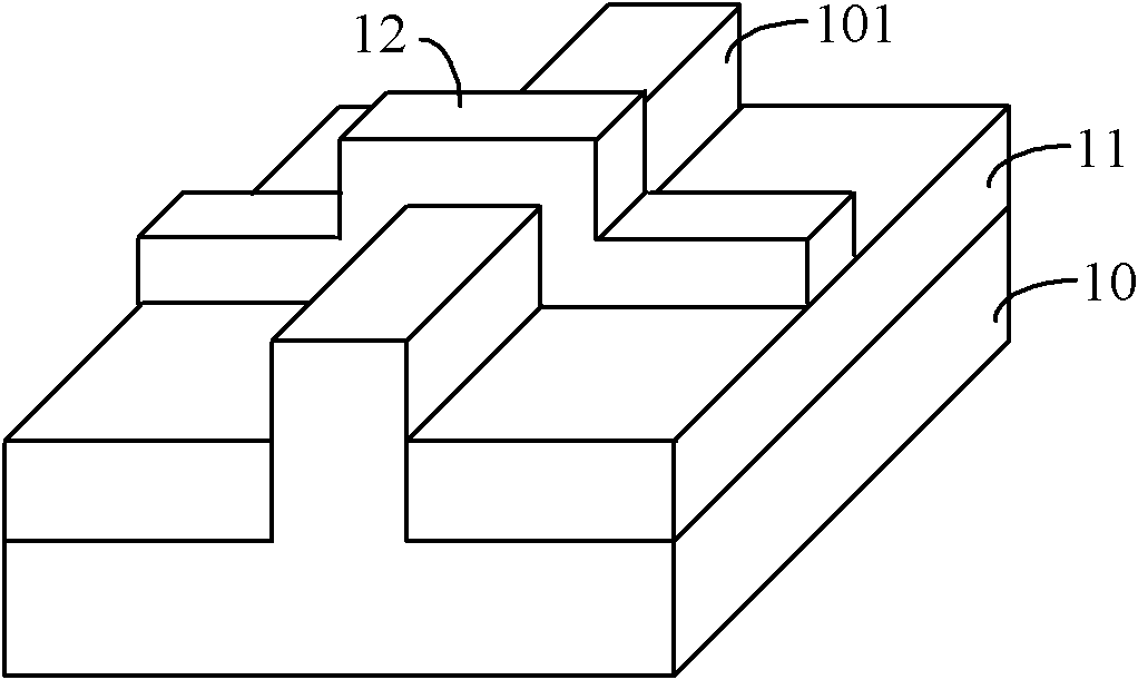
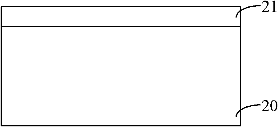
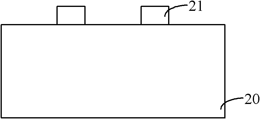
[0038] In the method for forming multi-gate devices in the prior art, chemical mechanical polishing is often used to planarize the surface of the dielectric layer covering the fins, and its local flatness is low, which affects the consistency of device performance.
[0039] In the method for forming a multi-gate device according to the embodiment of the present invention, a dielectric layer and a sacrificial layer are sequentially formed on the fin portion, and then the sacrificial layer is subjected to first reactive ion etching to expose the dielectric layer, and then the remaining sacrificial layer and dielectric layer are The layer is subjected to second reactive ion etching, wherein the etching rate of the sacrificial layer is lower than that of the dielectric layer in the second reactive ion etching, so as to obtain a surface of the dielectric layer with relatively high local flatness.
[0040] Further, the etching rate of the sacrificial layer by the second reactive ion ...
PUM
| Property | Measurement | Unit |
|---|---|---|
| Thickness | aaaaa | aaaaa |
Abstract
Description
Claims
Application Information
 - R&D Engineer
- R&D Manager
- IP Professional
- Industry Leading Data Capabilities
- Powerful AI technology
- Patent DNA Extraction
Browse by: Latest US Patents, China's latest patents, Technical Efficacy Thesaurus, Application Domain, Technology Topic, Popular Technical Reports.
© 2024 PatSnap. All rights reserved.Legal|Privacy policy|Modern Slavery Act Transparency Statement|Sitemap|About US| Contact US: help@patsnap.com