

Detection method of selective doping region property
A technology of doped regions and detection methods, applied in the field of solar cells, can solve the problem of unusable selective emitters, and achieve the effect of high resolution
- Summary
- Abstract
- Description
- Claims
- Application Information
AI Technical Summary
Problems solved by technology
Method used
Image

Examples
Embodiment 1
[0026] Example 1 Detects the characteristics of the selectively doped region made by gas diffusion + laser doping
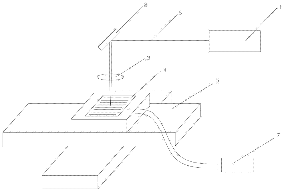
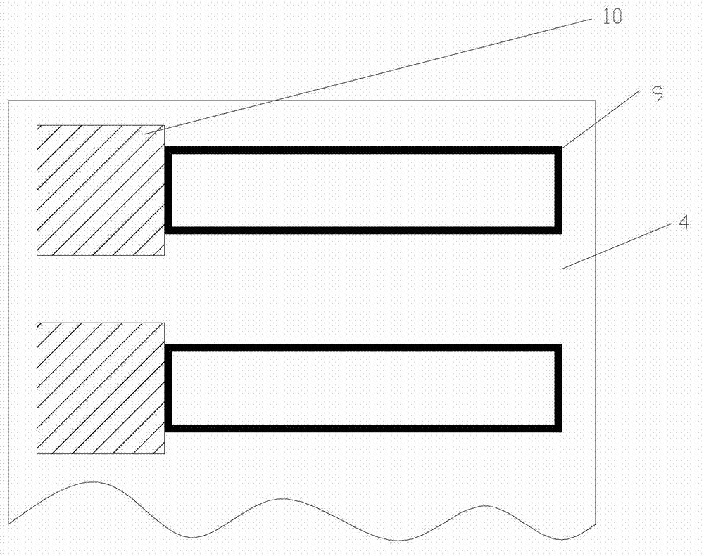
[0027] (1) The first low-doped gas diffusion is completed on the silicon wafer, and then the surface dielectric film is plated, and then a certain pattern of metal paste is printed on the surface of the silicon wafer according to the test requirements, and the metal electrode is formed after sintering. figure 2 As shown, each crystalline silicon wafer sample 4 is provided with a plurality of independent test areas, wherein each test area is provided with collected electrodes 9 and electrodes 10 connected to external circuits;
[0028] (2) Using the beam-induced current method (laser wavelength 532nm, the spot diameter of the focused laser beam is about 30gm), the focused laser beam is used to scan the surface of the battery, and at the same time, the photocurrent generated by the corresponding scanning point is measured through the electrodes to form the photogene...
Embodiment 2
[0033] Example 2 Detects the characteristics of the selectively doped region made by two gas diffusions
[0034] (1) Since electrodes cannot be made between the two gas diffusions, two adjacent silicon wafers cut from the middle of the same ingot can be used. It can be considered that the performance and internal characteristics of the silicon wafers are basically the same. If the silicon wafers are placed in the same position adjacent to the middle of the diffusion furnace, it can be considered that the diffusion process is basically the same, so that the performance difference between the two silicon wafers after diffusion is very small;
[0035](2) After the two silicon wafers complete a gas diffusion, one of them is used as a reference wafer to complete the coating, printing and sintering electrodes, such as figure 2 shown;
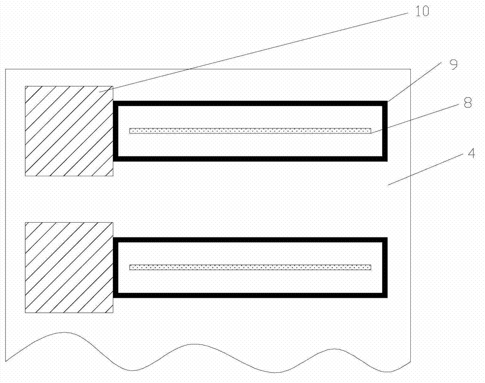
[0036] (3) The other piece is used as a test piece, and a mask is made on the surface according to the selective emitter pattern, and then the secon...
Embodiment 3
[0039] Example 3 Detecting the characteristics of the selectively doped region made by gas diffusion + doping slurry
[0040] (1) The first low-doped gas diffusion is completed on the silicon wafer, and then the surface dielectric film is plated, and then a certain pattern of metal paste is printed on the surface of the silicon wafer according to the test requirements, and the metal electrode is formed after sintering, such as figure 2 shown;
[0041] (2) As shown in Figure 1, using the beam-induced current method (laser wavelength is 633nm, spot diameter 50μm), the focused laser beam is used to scan the surface of the battery, and at the same time, the photocurrent generated by the corresponding scanning point is measured through the electrodes to form the test area. Detailed data and images of photogenerated current;
[0042] (3) Print the doping paste on the surface of the silicon wafer according to the pattern of the selective emitter by screen printing or precision print...
PUM
 Abstract
Description
Claims
Application Information