Method for manufacturing nonvolatile memory device, nonvolatile memory element, and nonvolatile memory device

A technology of non-volatile storage and manufacturing methods, applied in the field of non-volatile storage elements, capable of solving problems such as the easy deterioration of variable resistance elements, and achieving the effects of simplification of the manufacturing process, ease of control, and improvement of reliability

Active Publication Date: 2013-01-02
PANASONIC SEMICON SOLUTIONS CO LTD
View PDF11 Cites 12 Cited by
  • Summary
  • Abstract
  • Description
  • Claims
  • Application Information

AI Technical Summary

Problems solved by technology

As a result, there is a problem that the variable resistance ele

Method used


Image

  • Method for manufacturing nonvolatile memory device, nonvolatile memory element, and nonvolatile memory device
  • Method for manufacturing nonvolatile memory device, nonvolatile memory element, and nonvolatile memory device
  • Method for manufacturing nonvolatile memory device, nonvolatile memory element, and nonvolatile memory device

Examples


Embodiment approach 1

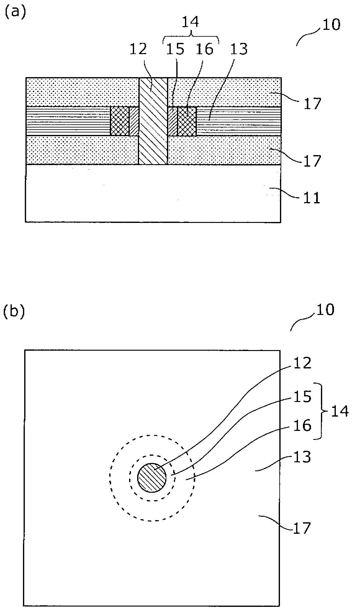
[0054] exist figure 1 represents the nonvolatile memory element according to Embodiment 1 of the present invention. figure 1 (a) is a sectional view of the nonvolatile memory element 10, figure 1 (b) is a plan view of the nonvolatile memory element 10 viewed from above (observed from a direction perpendicular to the substrate 11 ).

[0055] figure 1 The illustrated nonvolatile memory element 10 is composed of a substrate 11 , columnar electrodes 12 , a conductive layer 13 , a variable resistance layer 14 , and an interlayer insulating film 17 . The variable resistance layer 14 is composed of a first variable resistance layer 15 and a second variable resistance layer 16 .

[0056] Conductive layer 13 is formed parallel to the main surface of substrate 11 . The conductive layer 13 and a pair of interlayer insulating films 17 formed in contact with both surfaces (the upper surface and the lower surface) constitute a laminated body. The columnar electrode 12 is a columnar...

Embodiment approach 2

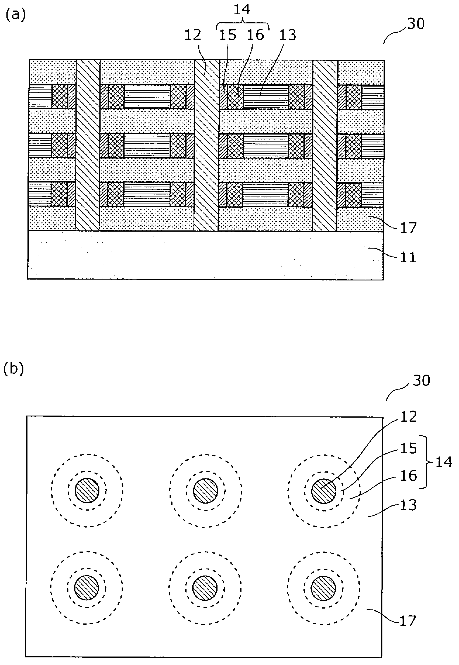
[0075] exist image 3 2 shows the nonvolatile memory device 30 according to Embodiment 2 of the present invention. image 3 (a) is a sectional view of the nonvolatile memory device 30, image 3 (b) is a plan view of the nonvolatile memory device 30 viewed from above (observed from a direction perpendicular to the substrate 11 ).

[0076] Such as image 3 (a), image 3 As shown in (b), the nonvolatile memory device 30 is formed by stacking three layers with 6 memory cells in each layer in the vertical direction (direction perpendicular to the substrate), and 18 memory cells as a whole. memory array in a 3-dimensional configuration. Here, the memory cell corresponds to the nonvolatile memory element 10 of Embodiment 1, and is composed of a columnar electrode 12 , a conductive layer 13 , a variable resistance layer 14 , and an interlayer insulating film 17 .

[0077] Also in the nonvolatile memory device 30, as in the first embodiment, after the contact hole is formed, the p...

Embodiment approach 3

[0082] Figure 5 A nonvolatile memory device 50 according to Embodiment 3 of the present invention is shown. The nonvolatile memory device 50 of Embodiment 3 is a modified example of the nonvolatile memory device 30 of Embodiment 2. As shown in FIG. Figure 5 (a) is a sectional view of the nonvolatile memory device 50, Figure 5 (b) is a plan view viewed from above (observed from a direction perpendicular to the substrate 11 ). Also in this third embodiment, as in the second embodiment, the process can be simplified, and the uniformity of the film thickness of the variable resistance layer 14 can be controlled.

[0083] The difference from Embodiment 2 is that, as Figure 5 (a), Figure 5 As shown in (b), the strip-shaped insulating layer 57 perpendicular to the main surface of the substrate 11 is formed in a columnar shape two-dimensionally arranged in the row direction and the column direction in a plane parallel to the main surface of the substrate 11 . The electrodes ...


PUM

PropertyMeasurementUnit
Specific resistanceaaaaaaaaaa

Abstract

Disclosed is a manufacturing method, whereby a nonvolatile memory device having a stable memory performance can be manufactured with a simple process. The method includes: a step wherein a laminated structure is formed by alternately laminating, on a substrate (11), a plurality of conductive layers (13) containing a transition metal, and a plurality of interlayer insulating films (17) composed of an insulating material; a step wherein a contact hole, which penetrates the laminated structure and exposes parts of the respective conductive layers (13) is formed; a step wherein the conductive layer (13) parts exposed in the contact hole are oxidized, and variable-resistance layers (14) wherein resistance values reversibly change on the basis of electrical signals transmitted thereto are formed; and a step wherein a conductive material is embedded in the contact hole, and a columnar electrode (12) connected to the variable-resistance layers (14) is formed in the contact hole.

Description

technical field [0001] The present invention relates to a variable resistance nonvolatile memory element whose resistance value changes reversibly upon application of an electrical signal, a nonvolatile memory device including the element, and a method for manufacturing the nonvolatile memory device. Background technique [0002] In recent years, with the development of digital technology in electrical equipment, there has been an increasing demand for large-capacity non-volatile storage devices in order to store data such as music, images, and information. As one countermeasure to meet such needs, a resistance variable layer whose resistance value changes due to an applied electric pulse and keeps its state is used for a nonvolatile memory device (hereinafter referred to as ReRAM) is attracting attention. This is because it has features such as relatively simple structure as a memory element, easy realization of high density, and easy compatibility with conventional semico...

Claims


Application Information

Patent Timeline
IPC IPC(8): H01L27/105G11C13/00H01L45/00
CPCH01L27/249H01L45/08H01L45/145H01L45/1675H01L27/2436H01L45/1633H01L27/24G11C13/0002H01L45/146H01L45/1226G11C2213/77H10B63/845H10B63/30H10N70/24H10N70/823H10N70/028H10N70/8833
Inventor 巍志强高木刚饭岛光辉
Owner PANASONIC SEMICON SOLUTIONS CO LTD
Why Eureka
Try Eureka