Method for producing composition for organic electroluminescent element, composition for organic electroluminescent element, method for producing organic electroluminescent element, organic electroluminescent element, organic el display device, and organic el lighting
An electroluminescent element and a manufacturing method technology, which are applied to semiconductor devices of light-emitting elements, electroluminescent light sources, electrical components, etc., can solve the problems of solute precipitation, agglomeration and crystallization, and achieve long driving life and high current efficiency. , the effect of high technical value
- Summary
- Abstract
- Description
- Claims
- Application Information
AI Technical Summary
Problems solved by technology
Method used
Image
Examples
Embodiment 1
[0421] {Example 1}
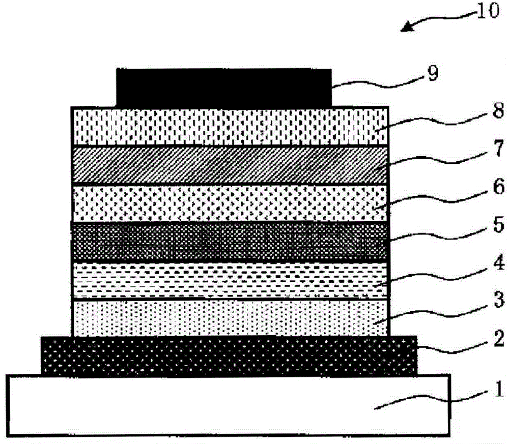
[0422] made as figure 1 The organic electroluminescence device shown. First, a transparent conductive film of ITO with a thickness of 150 nm is deposited on a glass substrate, and a pattern of 2 mm wide stripes is made to form the anode 2 of the ITO layer. Film-forming product) 1. After cleaning in the order of ultrasonic cleaning of surfactant aqueous solution, washing with ultrapure water, ultrasonic cleaning with ultrapure water, and washing with ultrapure water, use compressed air Dry, and finally perform ultraviolet ozone cleaning.
[0423] Next, 2.0% by weight of a hole-transporting polymer compound having a repeating structure shown in (P1) below, and 4-isopropyl-4'-methyldiphenyl 0.8 wt % ethyl benzoate solution of iodonium tetrakis(pentafluorophenyl) borate (composition for forming a hole injection layer).
[0424] [chem 22]
[0425]
[0426] The composition for forming a hole injection layer was formed into a film on the above-mentioned I...
Embodiment 2
[0454] {Example 2}
[0455] In Example 1, except for forming the light-emitting layer 5, the above-mentioned light-emitting material (C6), and the charge transport materials (C3) and (C4) shown below were used to form the light-emitting layer according to the composition shown below. Except for the composition, it was carried out in the same manner as in Example 1, and an element was produced.
[0456] [chem 26]
[0457]
[0458]
[0459]
Embodiment 3
[0460] {Example 3}
[0461] In Example 1, except for the formation of the light emitting layer 5, a composition for forming a light emitting layer was prepared by using the light emitting material (C8) shown below and the charge transport material (C5) shown below according to the composition shown below, and The baking time during wet film formation was set to 20 minutes to obtain a light emitting layer with a film thickness of 50 nm, and the device was produced in the same manner as in Example 1.
[0462] [chem 27]
[0463]
[0464]
[0465] Solvent cyclohexylbenzene
[0466] Component concentration C5: 3.3% by weight
[0467] C8: 0.33% by weight
PUM
 Abstract
Description
Claims
Application Information


