Method of testing storage array and control device

A storage array and control device technology, applied in the field of storage, can solve the problems of long testing time of storage arrays, and achieve the effects of shortening testing time and reducing sub-threshold current

Inactive Publication Date: 2013-01-09
SHANGHAI HUAHONG GRACE SEMICON MFG CORP
View PDF4 Cites 10 Cited by
  • Summary
  • Abstract
  • Description
  • Claims
  • Application Information

AI Technical Summary

Problems solved by technology

[0008] The present invention solves the problem of long testing time for testing a storage array composed of small-sized storage units

Method used


Image

  • Method of testing storage array and control device
  • Method of testing storage array and control device
  • Method of testing storage array and control device

Examples


Embodiment Construction

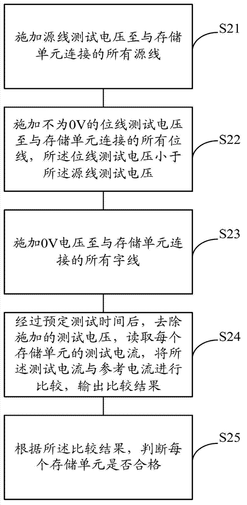
[0026] In order to make the above objects, features and advantages of the present invention more comprehensible, specific implementations of the present invention will be described in detail below in conjunction with the accompanying drawings and embodiments.

[0027] In the following description, many specific details are set forth in order to fully understand the present invention, but the present invention can also be implemented in other ways than those described here, so the present invention is not limited by the specific embodiments disclosed below.

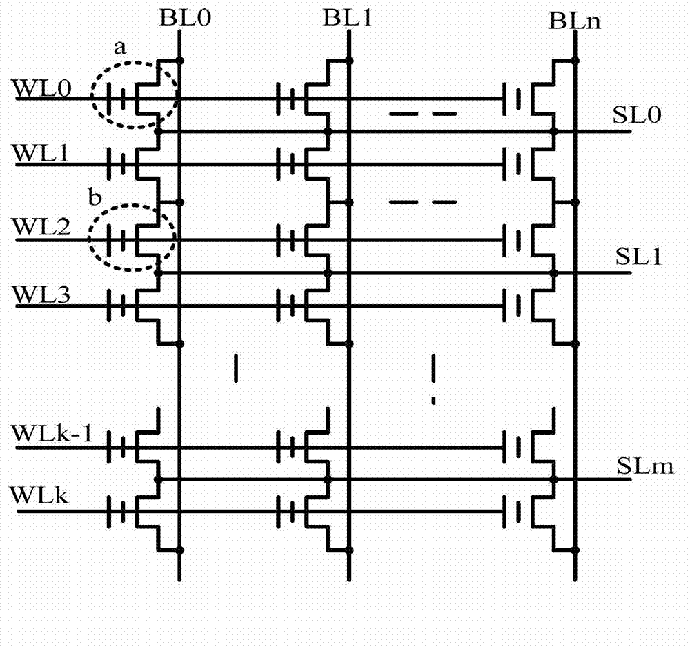
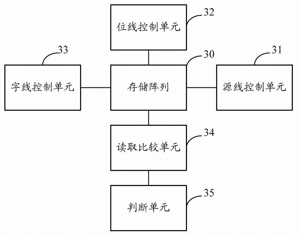
[0028]As described in the background technology, the memory array composed of small-sized memory cells is easily tested for column crosstalk. The prior art is carried out through the user mode. Since this test method needs to test each column of memory cells separately, it is different from the Very time consuming compared to conventional testing methods. Therefore, the inventor considers whether the conventional test meth...


PUM


Abstract

The invention discloses a method of testing a storage array and a control device. In the storage array, storage units in a same line share a bit line, storage units in a same row share a word line, and the storage units in every two rows share a same source line. The testing method comprises the following steps of: applying a source line testing voltage to all source lines connected with the storage units; applying a bit line testing voltage which is not equal to 0V to all bit lines connected with the storage units; applying a 0V voltage to all word lines connected with the storage units; after preset testing time, removing the applied testing voltage, reading a testing current of each storage unit, comparing the testing current with a reference current, and outputting a comparison result; and according to the comparison result, judging whether each storage unit is qualified or not, wherein the bit line testing voltage is smaller than the source line testing voltage. With the adoption of the method of testing the storage array and the control device provided by the technical scheme of the invention, the testing time of the storage array formed by storage units in a small size is reduced.

Description

technical field [0001] The invention relates to the field of memory technology, in particular to a method and a control device for testing memory cells prone to column crosstalk in a memory array. Background technique [0002] Due to its many advantages such as high speed, high density, shrinkability, and ability to retain data after power failure, non-volatile memory (NVM, Nonvolatile memory), as an integrated circuit storage device, is widely used in portable computers, mobile phones, In electronic products such as digital music players. Generally, according to the gate structure of the transistors that make up the storage unit, the structure of the non-volatile memory storage unit is divided into two types: stacked gate and split gate structure, in which the split gate storage unit effectively avoids over-erasing effect and has higher programming efficiency and has been widely used. [0003] figure 1 It is a structural schematic diagram of a split gate storage array, w...

Claims


Application Information

Patent Timeline
IPC IPC(8): G11C29/12
Inventor 杨光军胡剑
Owner SHANGHAI HUAHONG GRACE SEMICON MFG CORP
Why Eureka
Try Eureka