Semiconductor integrated circuits with power reduction mechanism

a technology of integrated circuits and power reduction mechanisms, applied in the field of semiconductor integrated circuits, can solve the problems of low operation speed, large transient current, and inability to minimize the threshold current in both standby mode and operating mode simultaneously, so as to minimize the leakage current flowing in the non-selected circuit, and reduce the total leakage current

Inactive Publication Date: 2005-01-04
PS4 LUXCO SARL
View PDF16 Cites 24 Cited by
  • Summary
  • Abstract
  • Description
  • Claims
  • Application Information

AI Technical Summary

Benefits of technology

The concept common to the semiconductor integrated circuit chips given in the summary of the invention is to have a plurality of circuit blocks and at least two circuit terminals through which a desired operating voltage is applied to these circuit blocks, and to have current control means provided for the subthreshold currents in the circuit blocks between each of the circuit blocks and at least one of the circuit terminals, so that the leakage current in a certain one of the circuit blocks is controlled by the current control means during a period including part of the time in which at least

Problems solved by technology

Therefore, the subthreshold currents in both the standby mode and the operating mode cannot be simultaneously minimized.
In FIG. 14, when each block is not selected, the power line of each block is at 0 V, and even when the block selecting operation is started, all the power lines for the nonselected blocks

Method used


Image

  • Semiconductor integrated circuits with power reduction mechanism
  • Semiconductor integrated circuits with power reduction mechanism
  • Semiconductor integrated circuits with power reduction mechanism

Examples


Embodiment Construction

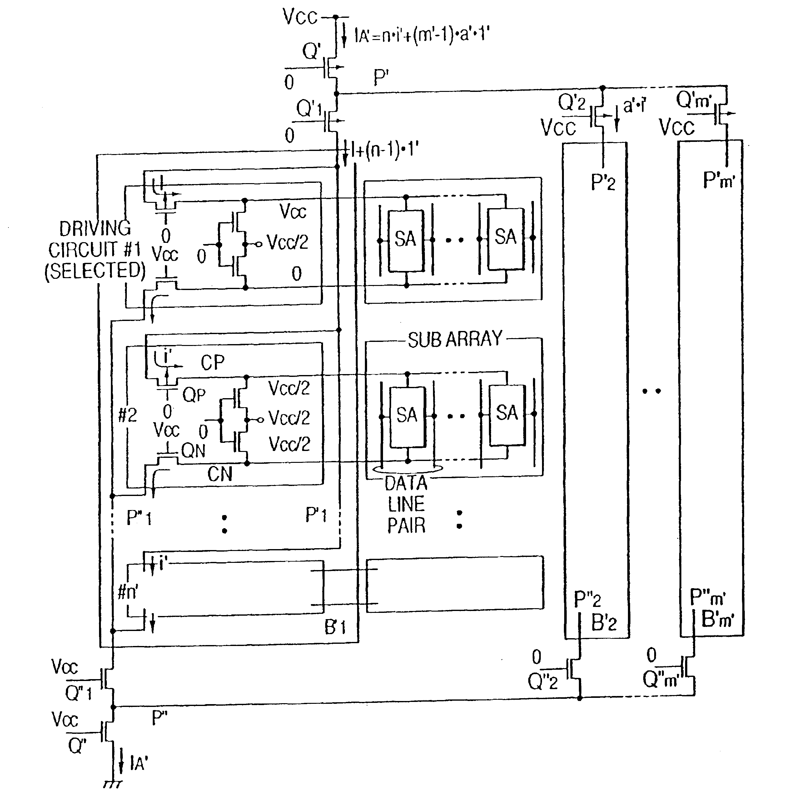
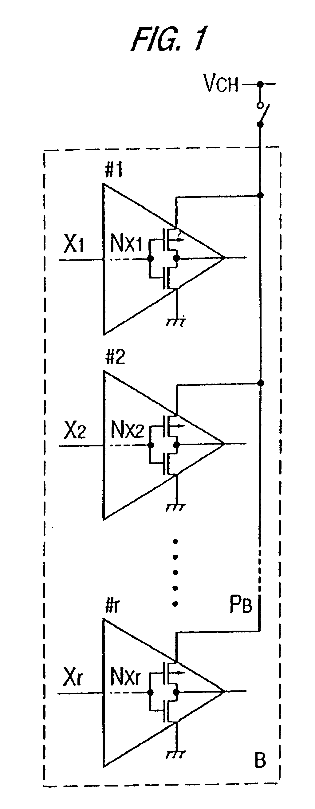
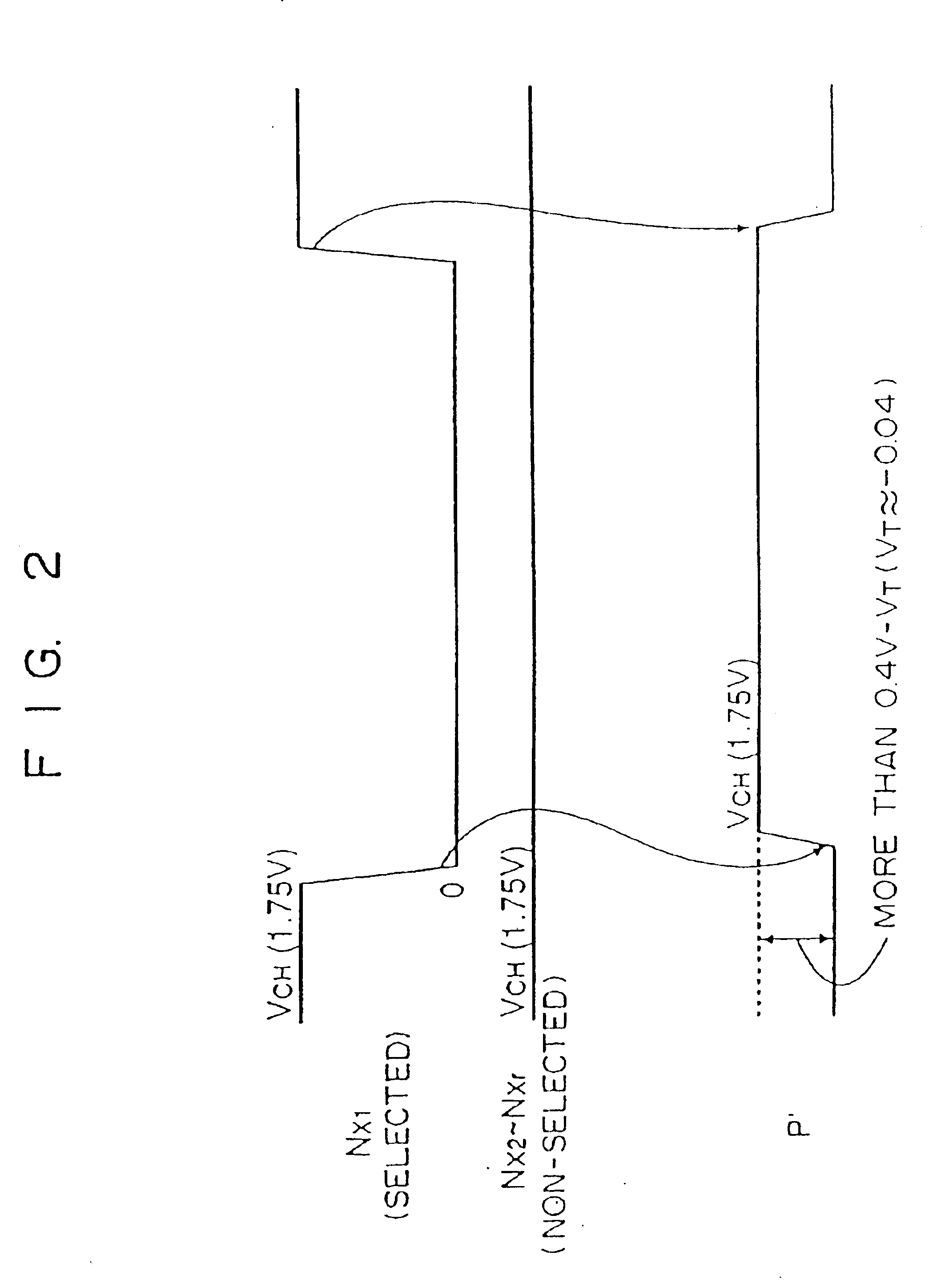
First, a description will be made of an application of the invention to a word driver (WD shown in FIG. 23) of DRAM. We consider the state after a word line has been selected and supplied with a necessary word voltage VCH. In the conventional arrangement shown in FIG. 24, if VT is only high enough, almost no subthreshold current flows in the source-drain paths of the MOS transistors of all CMOS drivers of which the gate-source voltages are substantially zero. However, when VT is reduced to about 0.4 V or below, the subthreshold current flows in the word drivers. As, the capacity becomes large and the word driver number (r) increases, the intensity of this current becomes significant. The total subthreshold current IA can be expressed as: IA=m·n·i=m·n·I0·WW0·10-VTS

where VT is the threshold voltage defined by the current value I0, and S is the subthreshold swing as shown in FIG. 22B. The word driver source VCH is normally produced by boosting the external source voltage within the chi...


PUM


Abstract

Power dissipation of a semiconductor integrated circuit chip is reduced when it is operated at an operating voltage of 2.5 V or below. A switching element is provided in each circuit block within the chip. Constants of the switching element are set so that leakage current in each switching element in their off-state is smaller than the subthreshold current of MOS transistors within the corresponding circuit block. Active current is supplied to active circuit blocks, while switching elements of non-active circuit blocks are turned off. Thus, dissipation currents of non-active circuit blocks are limited to leakage current value of corresponding switching elements. Thus, the sum of dissipation currents of non-active circuit blocks is made smaller than the active current in the active circuit blocks. As a result, power dissipation in the semiconductor integrated circuit chip can be reduced even in the active state.

Description

BACKGROUND OF THE INVENTION AND SUMMARY OF THE INVENTIONThe present invention relates to semiconductor integrated circuits suitable for high-speed and low-power operation, and particularly to a semiconductor integrated circuit formed of small-geometry MOS transistors.The semiconductor integrated circuits have so far been developed toward the scaling down of MOS transistors. However, since the minute structure of MOS transistors reduces their breakdown voltage the more as the degree of the minuteness becomes greater, the operating voltage of the small-geometry MOS transistors must be lowered, as described in International Symposium on VLSI Technology, Systems and Applications, Proceedings of Technical Papers, pp.188-192 (May 1989). The operating voltages of the semiconductors used in the battery-operated portable electronic apparatus must be further reduced for their low power consumption.In order to maintain their high-speed operation under reduced operating voltages, it is also nec...

Claims


Application Information

Patent Timeline
IPC IPC(8): G11C5/14G11C8/00G11C7/06G11C8/08G11C8/12H03K19/00H03K19/003
CPCG11C5/147G11C7/065G11C8/08G11C8/12H03K19/00361G11C11/4074H03K19/0016H03K19/0027G11C8/18
Inventor SAKATA, TAKESHIITOH, KIYOOHORIGUCHI, MASASHI
Owner PS4 LUXCO SARL
Why Eureka
Try Eureka