Organic semiconductor film and method for manufacturing the same, and stamp for contact printing

An organic semiconductor film, organic semiconductor technology, applied in semiconductor/solid-state device manufacturing, semiconductor devices, transistors, etc., can solve the problem of unimproved mobility, and achieve the effect of improving semiconductor characteristics and large charge mobility

Inactive Publication Date: 2013-01-09
TEIJIN LTD
View PDF12 Cites 2 Cited by
  • Summary
  • Abstract
  • Description
  • Claims
  • Application Information

AI Technical Summary

Problems solved by technology

However, the technology described in Patent Document 4 is a technology for reducing the leakage current and improving the on-off ratio by forming regions with different mobility in the organic semiconductor layer, but compared with the conventional organic semiconductor layer, the mobility The rate probably did not increase

Method used


Image

  • Organic semiconductor film and method for manufacturing the same, and stamp for contact printing
  • Organic semiconductor film and method for manufacturing the same, and stamp for contact printing
  • Organic semiconductor film and method for manufacturing the same, and stamp for contact printing

Examples


Embodiment

[0174] The present invention is described in detail using the following examples. However, the present invention is not limited thereto. In addition, the evaluation methods used in the following examples are as follows.

[0175] Water contact angle:

[0176] Using a CA-X water contact angle meter manufactured by Kyowa Interface Science (Kyowa Interface Science), the water contact angle was measured with pure water at 25°C.

[0177] Relative X-ray reflection peak height:

[0178] Using RINT TTR II manufactured by Rigaku, under the conditions of X-ray source Cu-Kα line and rotating counter cathode 50kV-300mA (15kW), the peak height of the symmetrical reflection of X-rays of organic semiconductor films was measured. The peak height was evaluated based on the relative height after normalizing to the same thickness with the peak height of the organic semiconductor film of the material produced by spin coating on the silicon wafer as a reference (according to Example 12 (comparis...

example 1

[0185] (Making impressions for contact printing)

[0186] As an impression material, a silicone rubber (SIM-260 manufactured by Shin-Etsu Chemical Co., Ltd.) was hardened into a flat plate, and oligomers were removed with hexane.

[0187] The impression material is cut into 20 mm squares, and a mask corresponding to the transfer portion is placed on the impression material to shield the transfer portion, and UV (ultraviolet ray) is applied to the impression material thus shielded for 30 minutes. ) - ozone treatment. That is, UV-ozone treatment was not performed on the transfer portion, but UV-ozone treatment was performed on the peripheral portion. After this UV-ozone treatment, a lyophilic surface is provided to the peripheral portion.

[0188] The water contact angle of the transfer part without UV-ozone treatment was 110°, and the water contact angle of the peripheral part subjected to UV-ozone treatment for 30 minutes was 44°. In addition, there were 12 transfer parts on...


PUM

PropertyMeasurementUnit
thicknessaaaaaaaaaa
thicknessaaaaaaaaaa
thicknessaaaaaaaaaa

Abstract

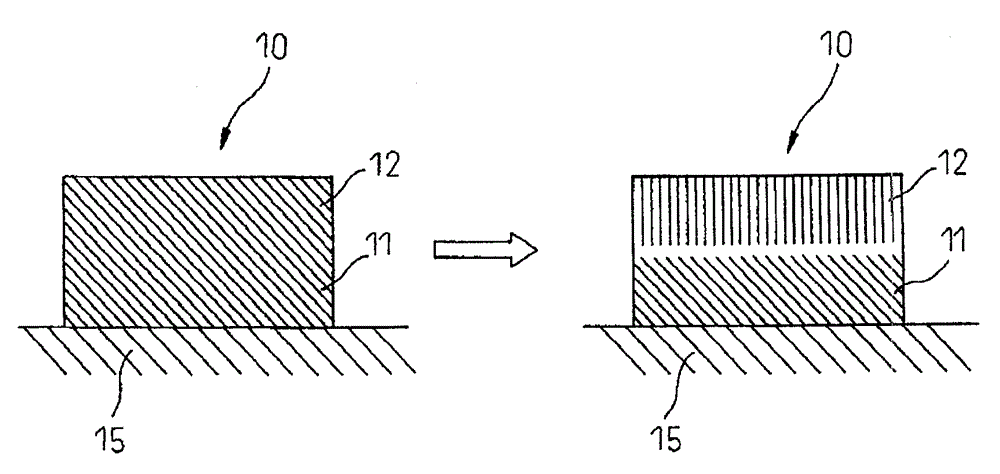
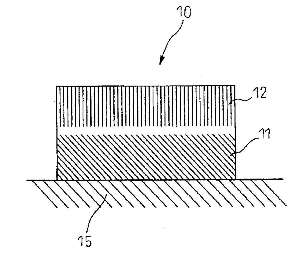
Disclosed is an organic semiconductor film (10) which has a value of 1 or more but less than 10 for the ratio of the charge mobility [(charge mobility of the surface side having larger charge mobility)/(charge mobility of the surface side having smaller charge mobility)] of two opposing surface sides (11, 12). In addition, the organic semiconductor film (10) has a relative X-ray reflectance peak height of 2.0 or more with respect to the peak height of an organic semiconductor film which has the same thickness and materials and is manufactured by performing spin coating on a silicon wafer. Alternatively, the organic semiconductor film (10) has a value of 2 or more for the ratio of the charge mobility [(charge mobility of the surface side having larger charge mobility)/(charge mobility of the surface side having smaller charge mobility)] of the two opposing surface sides (11, 12).

Description

technical field [0001] The first and second present inventions relate to a novel organic semiconductor film, a method for producing the same, and an organic semiconductor device and electric circuit having the organic semiconductor film. [0002] The third invention relates to a novel stamp for contact printing, particularly a stamp for contact printing used for producing an organic semiconductor film, and a method for producing an organic semiconductor film using the stamp for contact printing. Background technique [0003] In recent years, semiconductor films have been used in various applications such as semiconductor elements represented by thin film transistors (TFTs) and solar cells. [0004] Inorganic semiconductor films mainly used at present, especially inorganic semiconductor films using silicon as a semiconductor material, are manufactured using vacuum processes such as chemical vapor phase growth (CVD) and sputtering (sputtering), so the manufacturing cost is hig...

Claims


Application Information

Patent Timeline
Patent Type & Authority Applications(China)
IPC IPC(8): H01L21/368H01L21/336H01L29/786H01L51/05
CPCH01L51/0545H01L51/0004H01L51/0039H01L51/0512H01L51/0558H01L51/0036H10K71/13H10K85/115H10K85/113H10K10/484H10K10/466H10K10/462H10K10/464
Inventor 串田尚内藤裕义
Owner TEIJIN LTD
Why Eureka
Try Eureka