Method for manufacturing semiconductor device

A manufacturing method and semiconductor technology, applied in the fields of semiconductor/solid-state device manufacturing, semiconductor devices, lighting devices, etc., can solve problems such as changes in electrical characteristics of transistors, changes in electrical rate, etc.

Active Publication Date: 2013-01-09
SEMICON ENERGY LAB CO LTD
View PDF7 Cites 5 Cited by
  • Summary
  • Abstract
  • Description
  • Claims
  • Application Information

AI Technical Summary

Problems solved by technology

[0006] However, when hydrogen or moisture used to form an electron donor is mixed into the oxide semiconductor during the device manufacturing process, it may cause changes in conductivity
This phenomenon is the main cause of fluctuations in the electrical characteristics of transistors using oxide semiconductors

Method used


Image

  • Method for manufacturing semiconductor device
  • Method for manufacturing semiconductor device
  • Method for manufacturing semiconductor device

Examples


Embodiment approach 1

[0078] In this embodiment, refer to Figures 1A to 1C , Figures 2A to 2G , Figure 3A to Figure 3D A semiconductor device and a method of manufacturing the semiconductor device will be described.

[0079]

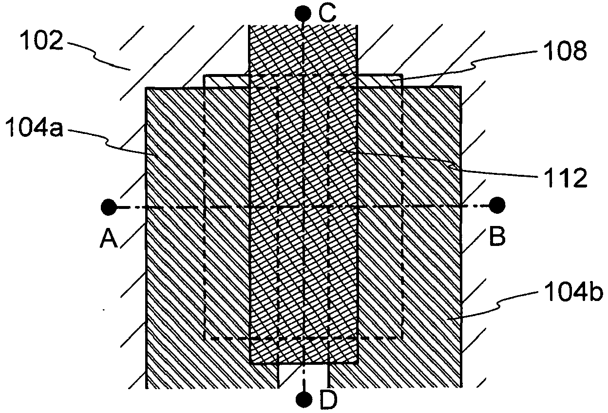
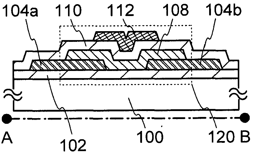
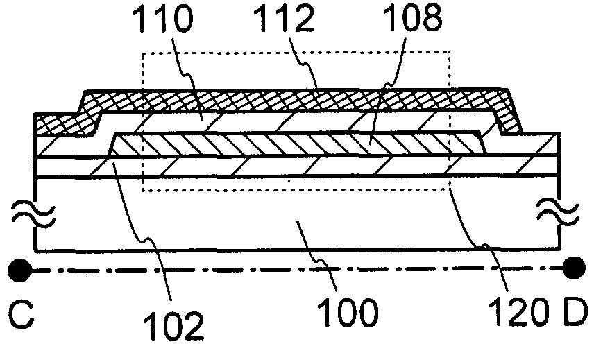
[0080] Figures 1A to 1C A structural example of the transistor 120 is shown. here, Figure 1A is a planar graph, and Figure 1B and Figure 1C respectively along the Figure 1A The cross-sectional views of the A-B section and the C-D section in the figure. Note that in Figure 1A In order to avoid complexity, some components of the transistor 120 (for example, the gate insulating film 110 ) are omitted.

[0081] Figures 1A to 1C The illustrated transistor 120 includes: an insulating film 102 over a substrate 100 ; a source electrode 104 a ; a drain electrode 104 b ; an oxide semiconductor film 108 ; a gate insulating film 110 ;

[0082] exist Figures 1A to 1C In the illustrated transistor 120 , the oxide semiconductor film 108 is an oxide semiconductor fil...

Embodiment approach 2

[0159] In this embodiment, refer to Figures 4A to 4F and Figure 5A to Figure 5C Another example of a method of manufacturing a semiconductor device will be described.

[0160]

[0161] The structure of the semiconductor device manufactured by the manufacturing method of this embodiment is the same as that of the transistor 120 of the above-mentioned embodiment. That is, the semiconductor device includes: an insulating film 102 on a substrate 100; a source electrode 104a; a drain electrode 104b; an oxide semiconductor film 108; a gate insulating film 110; Figures 1A to 1C ).

[0162] As described in the above embodiments, in the transistor 120 , the oxide semiconductor film 108 is an oxide semiconductor film subjected to an oxygen doping process. In addition, in this embodiment, oxygen doping treatment is also performed on the insulating film 102 and the gate insulating film 110 . Through the oxygen doping treatment described above, the transistor 120 with further impr...

Embodiment approach 3

[0237] In this embodiment, refer to Figures 6A to 6F Another example of a method of manufacturing a semiconductor device will be described.

[0238]

[0239] The structure of the semiconductor device manufactured by the manufacturing method of this embodiment is the same as that of the transistor 120 of the above-mentioned embodiment. That is, the semiconductor device includes: an insulating film 102 on a substrate 100; a source electrode 104a; a drain electrode 104b; an oxide semiconductor film 108; a gate insulating film 110; Figures 1A to 1C ).

[0240] As described in the above embodiments, in the transistor 120 , the oxide semiconductor film 108 is an oxide semiconductor film subjected to an oxygen doping process. In addition, in this embodiment, oxygen doping treatment is also performed on the insulating film 102 and the gate insulating film 110 . Through the oxygen doping treatment described above, the transistor 120 with further improved reliability can be reali...


PUM


Abstract

One object of one embodiment of the present invention is to provide a highly reliable semiconductor device including an oxide semiconductor, which has stable electrical characteristics. In a method for manufacturing a semiconductor device, a first insulating film is formed; source and drain electrodes and an oxide semiconductor film electrically connected to the source and drain electrodes are formed over the first insulating film; heat treatment is performed on the oxide semiconductor film so that a hydrogen atom in the oxide semiconductor film is removed; oxygen doping treatment is performed on the oxide semiconductor film, so that an oxygen atom is supplied into the oxide semiconductor film; a second insulating film is formed over the oxide semiconductor film; and a gate electrode is formed over the second insulating film so as to overlap with the oxide semiconductor film.

Description

technical field [0001] The present invention relates to a semiconductor device and a method for manufacturing the semiconductor device. [0002] In this specification, a semiconductor device refers to all devices that can operate by utilizing semiconductor characteristics, and thus electro-optical devices, semiconductor circuits, and electronic equipment are all semiconductor devices. Background technique [0003] A technique of constituting a transistor using a semiconductor thin film formed on a substrate having an insulating surface has attracted attention. The transistor is widely used in electronic devices such as integrated circuits (ICs) and image display devices (display devices). Silicon-based semiconductor materials are widely known as semiconductor thin films that can be applied to transistors. However, oxide semiconductors are attracting attention as other materials. [0004] For example, it has been disclosed that the active layer of a transistor uses an elec...

Claims


Application Information

Patent Timeline
Patent Type & Authority Applications(China)
IPC IPC(8): H01L29/786H01L21/336H05B44/00
CPCH01L29/78603H01L29/78H01L29/7869H01L29/4908H01L27/1225H01L21/383H01L29/66742H01L21/477H01L29/263H01L29/66969H01L27/1255
Inventor 山崎舜平
Owner SEMICON ENERGY LAB CO LTD
Why Eureka
Try Eureka