Method capable of improving uniformity of porous silicon film physical micro-structure and optical characteristics

A technology of optical properties and porous silicon, which is applied in the directions of microstructure technology, microstructure devices, and manufacturing microstructure devices, etc., can solve the problems of uneven physical microstructure and optical properties of porous silicon films, and achieve the effect of improving uniformity.

Inactive Publication Date: 2013-01-16
HUNAN UNIV OF ARTS & SCI
View PDF4 Cites 11 Cited by
  • Summary
  • Abstract
  • Description
  • Claims
  • Application Information

AI Technical Summary

Problems solved by technology

[0003] In order to overcome the current galvanostatic corrosion method used in the preparation of porous silicon films, the physical microstructure and optical properties of the porous silicon films along the longitudinal direction are not uniform, so that the prepared porous silicon single-layer film and the microstructure composed of porous silicon multi-layer film The above-mentioned defect of cavity; The purpose of this invention is: provide a kind of new method that can improve the uniformity of physical microstructure and optical characteristic of porous silicon thin film, in order to improve the vertical physical microstructure of porous silicon thin film and optical characteristic keep uniform, improve porous silicon thin film. Optical Properties of Silicon Monolayer Film and Bragg Mirror and Microcavity Composed of Porous Silicon Multilayer Film

Method used


Image

  • Method capable of improving uniformity of porous silicon film physical micro-structure and optical characteristics

Examples


Embodiment 1

[0018] Embodiment one: the method (1) that can improve the uniformity of the physical microstructure of the porous silicon film, it comprises the following steps:

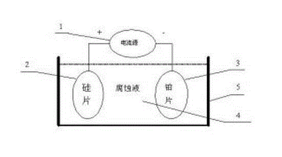
[0019] (1) Connect the circuit as shown in the attached drawing: that is, put the etching solution 4 in the etching tank 5, set the silicon chip 2 at one end of the etching tank, and set the platinum chip 3 at the other end of the etching tank, and the silicon chip 2 and the platinum sheet 3 are immersed in the etching solution 4, and a current source 1 is provided outside the etching tank, the positive pole of the current source is connected to the silicon wafer 2 through a wire, and the negative electrode of the current source is connected to the platinum sheet 3 through a wire;

[0020] (2) The type of silicon chip is P100, the resistivity is 0.01Ω.cm, the silicon chip is used as the anode of electrochemical corrosion, and the thin platinum sheet is used as the cathode of electrochemical corrosion; the silicon c...

Embodiment 2

[0027] Embodiment two: the method (two) that can improve the uniformity of the physical microstructure of the porous silicon film, it comprises the following steps:

[0028] (1) Connect the circuit as shown in the attached figure, that is, put the etching solution 4 in the etching tank 5, set the silicon wafer 2 at one end of the etching tank, and set the platinum wafer 3 at the other end of the etching tank, and the silicon wafer 2 and the platinum sheet 3 are immersed in the etching solution 4, and a current source 1 is provided outside the etching tank, the positive pole of the current source is connected to the silicon wafer 2 through a wire, and the negative electrode of the current source is connected to the platinum sheet 3 through a wire; wherein the current The decreasing corrosion current of the source is completed under computer control;

[0029] (2) The silicon wafer is selected as a P-type silicon wafer, and the resistivity is 0.007~0.01Ω.cm. The corrosion solutio...


PUM

PropertyMeasurementUnit
electrical resistivityaaaaaaaaaa
thicknessaaaaaaaaaa
electrical resistivityaaaaaaaaaa

Abstract

Provided is a method capable of improving uniformity of a porous silicon film physical micro-structure and optical characteristics. By reducing corrosion current density gradually, vesicularity in the longitudinal direction is reduced or refractive index is increased, increased vesicularity or reduced refractive index caused by increasing of corrosion depth is offset under the condition of constant corrosion current, so that a dynamic balancing state of the vesicularity and the refractive index is achieved, the uniformity of the physical micro-structure along the longitudinal direction of the porous silicon film and the optical characteristics is improved. The method has the advantages of improving the uniformity of the porous silicon film longitudinal physical micro-structure and the optical characteristics by reducing corrosion current density gradually so as to improve the uniformity of the physical micro-structure and the optical characteristics along the longitudinal direction; being favorable for building smooth level among multi-layer film interfaces of porous silicon; and being favorable for exploring an achieving scheme of a porous silicon multi-layer film with improved use uniformity and interface smooth level in photonic devices such as Prague reflectors and micro-cavities and achieving any wavelength hot shot of porous silicon micro-cavities possibly.

Description

technical field [0001] The invention relates to the field of semiconductor materials, in particular to a method capable of improving the uniformity of the physical microstructure and optical properties of a porous silicon thin film. Background technique [0002] Since the photoluminescence phenomenon of porous silicon at room temperature was reported by Camham in 1990, due to the special microstructure, physical properties, optical properties and electrical properties of porous silicon, porous silicon has stimulated research interests in many applications, such as luminescence Devices, sensors, and optical microcavities composed of multi-layer dielectric films; at present, research and production units in the industry generally use galvanostatic corrosion methods to prepare porous silicon single-layer films and porous silicon multi-layer films. formed microcavities. The experiment found that: ① porous silicon film has a very complex longitudinal microstructure; ② the micros...

Claims


Application Information

Patent Timeline
Patent Type & Authority Applications(China)
IPC IPC(8): B81C1/00
Inventor 龙永福张晋平雷立云胡惟文曹斌芳张爱龙王津彭元杰
Owner HUNAN UNIV OF ARTS & SCI
Why Eureka
Try Eureka