Full adder circuit and chip

A full adder and circuit technology, applied in the field of electronics, can solve the problem of the size limitation of MOS tube storage devices, and achieve the effects of programmable performance, low power consumption, and high storage density

Active Publication Date: 2013-01-16
PEKING UNIV
View PDF5 Cites 17 Cited by
  • Summary
  • Abstract
  • Description
  • Claims
  • Application Information

AI Technical Summary

Problems solved by technology

[0002] The full adder circuit is usually based on metal-oxide-semiconductor (MOS, Metal-Oxide-Semiconductor) tube storage devices. With the increasing requirements for chip integration, the size of the full adder circuit is also decreasing, but Due to the limitation of the size of the MOS transistor storage device itself, the full adder circuit in the prior art has the smallest size technology node

Method used


Image

  • Full adder circuit and chip
  • Full adder circuit and chip
  • Full adder circuit and chip

Examples


Embodiment Construction

[0027] The technical solutions in the embodiments of the present invention will be clearly and completely described below in conjunction with the accompanying drawings in the embodiments of the present invention. Obviously, the described embodiments are only some, not all, embodiments of the present invention. Based on the embodiments of the present invention, all other embodiments obtained by persons of ordinary skill in the art without creative efforts fall within the protection scope of the present invention.

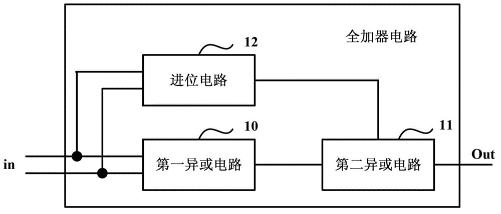
[0028] Such as figure 1 Shown is a schematic diagram of the composition and structure of the full adder circuit in an embodiment of the present invention.

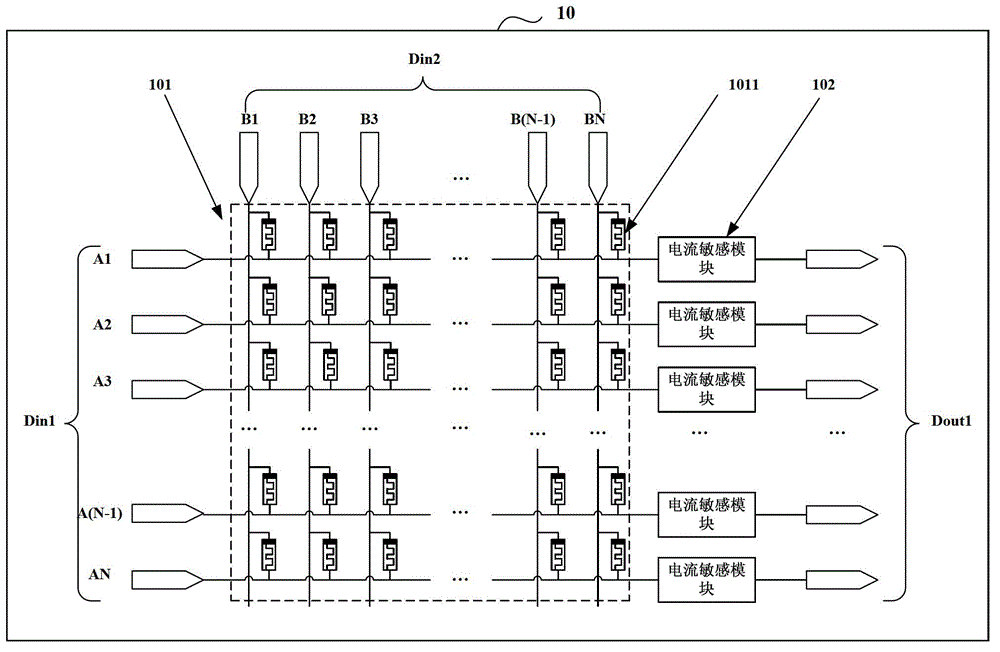
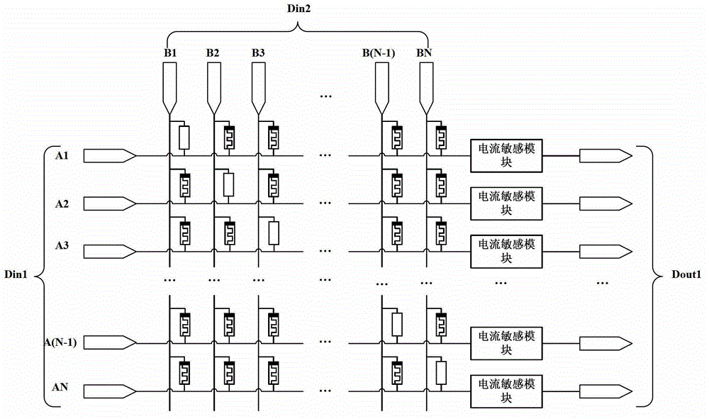
[0029]The full adder circuit can include a first exclusive OR circuit 10, a second exclusive OR circuit 11 and a carry circuit 12, wherein the input terminal of the first exclusive OR circuit 10 can be used as the signal input terminal in of the full adder circuit Receive two N-bit digital input signals for addi...


PUM


Abstract

The embodiment of the invention discloses a full adder circuit and a chip. The circuit comprises a first xor circuit, a second xor circuit and a carry circuit; the input end of the first xor circuit is used as the signal input end of the full adder circuit; a group of input ends of the second xor circuit are connected with the output end of the first xor circuit, the other group of input ends of the second xor circuit are used as the carry input ends of the full adder circuit, and the output end of the second xor circuit is used as the signal output end of the full adder circuit; the input end of the carry circuit is used as the signal input end of the full adder circuit, and the output end of the carry circuit is connected with the carry input end of the full adder circuit; and at least one of the first xor circuit, the second xor circuit and the carry circuit comprises a resistance-variable memristor array. In the embodiment of the invention, the area occupied by the full adder circuit is reduced, and meanwhile, the programmable performance of the full adder circuit is achieved.

Description

technical field [0001] The invention relates to the field of electronic technology, in particular to a full adder circuit and a chip. Background technique [0002] The full adder circuit is usually based on metal-oxide-semiconductor (MOS, Metal-Oxide-Semiconductor) tube storage devices. With the increasing requirements for chip integration, the size of the full adder circuit is also decreasing, but Due to the limitation of the size of the MOS transistor storage device itself, the full adder circuit in the prior art has a technology node with the smallest size. Contents of the invention [0003] The embodiment of the present invention provides a full adder circuit and a chip to solve the problem that the full adder circuit in the prior art has a minimum size technology node. [0004] In order to solve the above problems, the embodiment of the present invention discloses the following technical solutions: [0005] On the one hand, a full adder circuit is provided, includin...

Claims


Application Information

Patent Timeline
Patent Type & Authority Applications(China)
IPC IPC(8): H03K19/20
Inventor 黄如张耀凯蔡一茂陈诚
Owner PEKING UNIV
Why Eureka
Try Eureka