III-series nitride semiconductor device and manufacturing method thereof

A nitride semiconductor and nitride technology, applied in the field of microelectronics, can solve the problems of increased leakage, current collapse, and current collapse effect of gallium nitride devices, and achieve the effect of reducing the current collapse effect

Active Publication Date: 2013-01-30
ENKRIS SEMICON
View PDF5 Cites 17 Cited by
  • Summary
  • Abstract
  • Description
  • Claims
  • Application Information

AI Technical Summary

Problems solved by technology

These defects and impurities will greatly reduce the performance of the device, because dislocations and carbon impurities can introduce deep energy levels in the forbidden band, form trap centers or charge trapping centers, and trap charges in the nitride channel layer, lead to severe current collapse effect
On the other hand, oxygen and carbon introduced by unintentional doping and intrinsic defects including nitrogen defects will increase the leakage of gallium nitride devices during operation
In order to r

Method used


Image

  • III-series nitride semiconductor device and manufacturing method thereof
  • III-series nitride semiconductor device and manufacturing method thereof
  • III-series nitride semiconductor device and manufacturing method thereof

Examples


Example Embodiment

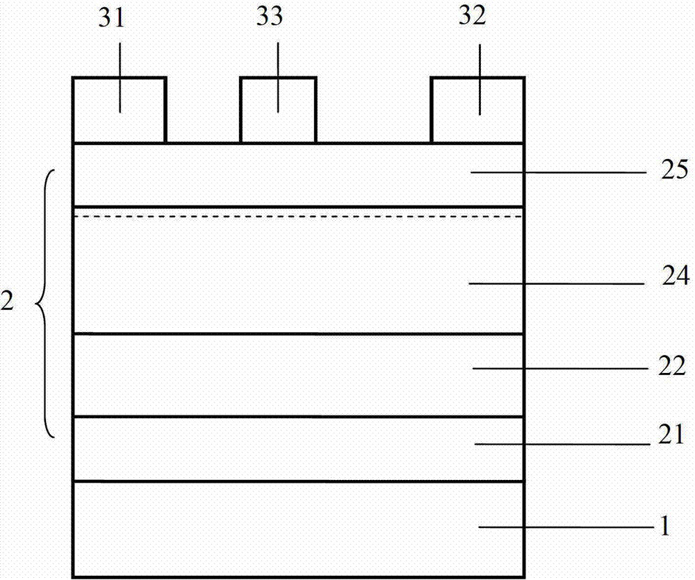
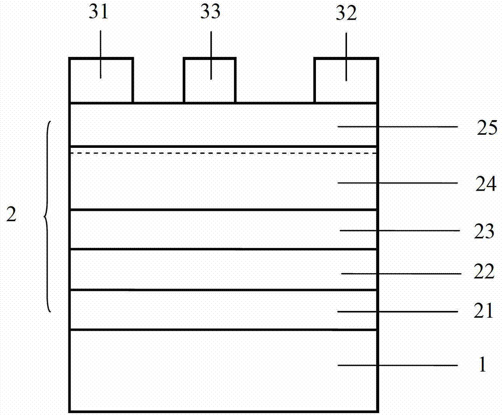
[0048] A group III nitride semiconductor device of the present invention includes:

[0049] Substrate

[0050] Nitride nucleation layer on the substrate;

[0051] A nitride buffer layer on the nitride nucleation layer;

[0052] A wide band gap and deep level modulation layer on the nitride buffer layer;

[0053] Nitride channel layer located on the wide band gap deep level modulation layer;

[0054] And an electrode formed on the nitride channel layer;

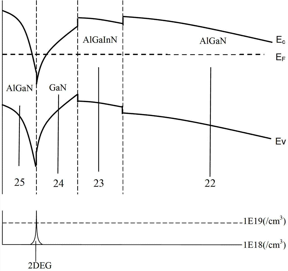
[0055] Wherein, the wide-bandgap deep-level modulation layer is formed of a group III nitride semiconductor layer containing deep-level defects, and the concentration of the deep-level defects is a constant or from a nitride buffer layer to a nitride channel layer Gradually decrease; the forbidden band width of the wide band gap and deep level modulation layer is larger than the band gap of the nitride channel layer.

[0056] Correspondingly, a method for manufacturing a group III nitride semiconductor device includes the following steps:...


PUM


Abstract

The invention discloses an III-series nitride semiconductor device and a manufacturing method thereof. The III-series nitride semiconductor device comprises a substrate, a nitride nucleating layer located on the substrate, a nitride buffering layer located on the nitride nucleating layer, a wide band gap deep-energy-grade modulating layer located on the nitride buffering layer, a nitride channel layer located on the wide band gap deep-energy-grade modulating layer, and an electrode formed on the nitride channel layer, wherein the wide band gap deep-energy-grade modulating layer is formed by an III-series nitride semiconductor layer containing a deep-energy-grade defect; the concentration of the deep-energy-grade defect is a constant or is gradually reduced from the nitride buffering layer to the nitride channel layer; and the wide band gap width of the wide band gap deep-energy-grade modulating layer is greater than the wide band gap width of the nitride channel layer. According to the III-series nitride semiconductor device and the manufacturing method thereof, the wide band gap deep-energy-grade modulating layer is inserted between the nitride channel layer and the nitride buffering layer, so as to play the roles of controlling leaked current and reducing a current collapsing effect.

Description

technical field [0001] The invention relates to the technical field of microelectronics, in particular to a Group III nitride semiconductor device and a manufacturing method thereof. Background technique [0002] Group III nitride semiconductors have the characteristics of large band gap, high dielectric breakdown electric field and high electron saturation drift rate, and are suitable for making high-frequency, high-temperature, high-speed switching and high-power electronic devices. On the one hand, due to the extremely high mobility and saturation rate of GaN, GaN electronic devices have good application prospects in high-frequency power amplifiers. From the 1990s to the present, the development of GaN-based radio frequency devices has been one of the hot spots in the research of GaN electronic devices. On the other hand, GaN-based power switching devices have received more and more attention in recent years. This is because gallium nitride is a wide bandgap semiconduct...

Claims


Application Information

Patent Timeline
IPC IPC(8): H01L29/06H01L29/778H01L21/335
Inventor 程凯
Owner ENKRIS SEMICON
Why Eureka
Try Eureka