

Semiconductor chip package structure
A chip packaging structure, semiconductor technology, applied in the direction of semiconductor devices, semiconductor/solid-state device components, electric solid-state devices, etc., can solve problems such as difficulties, achieve the effect of reducing parasitic capacitance and weakening the effect of current collapse
- Summary
- Abstract
- Description
- Claims
- Application Information
AI Technical Summary
Problems solved by technology
Method used
Image

Examples
Embodiment Construction
[0025] The preferred embodiments of the present invention will be described in detail below in conjunction with the accompanying drawings.
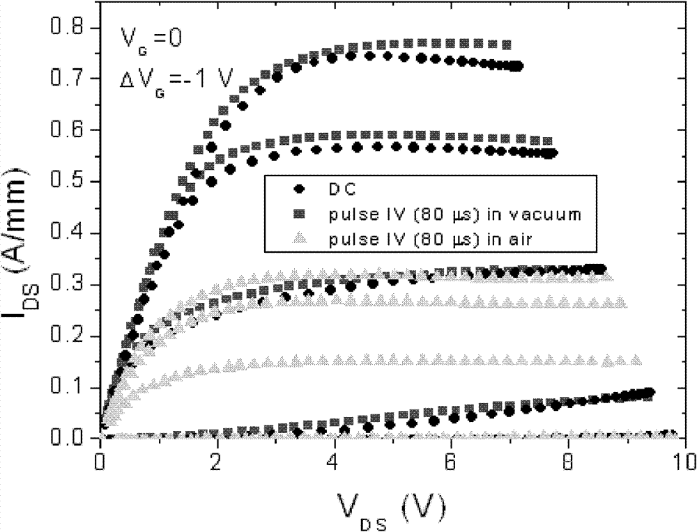
[0026] figure 1 shows the 80-µs pulsed current-voltage measurements of an AlGaN / GaN high electron mobility transistor with a 2nm SiN passivation layer in air (triangle markers) and vacuum (square markers), and also shows the dc Current and voltage measurement results (circle markers). Among them, the source-drain current (IDS) is used as a function of the source-drain voltage (VDS), and the gate voltage VG corresponding to the DC and 80 microsecond pulse current voltage is measured from the off state (-4V) to 0V, and the step size is 1V (VG= -4, -3, -2, -1, 0V). figure 1 It shows that there is a large DC-RF current collapse effect in the air environment, but there is no current collapse effect in the vacuum environment.
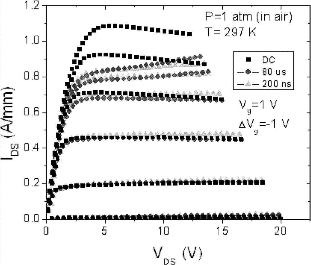
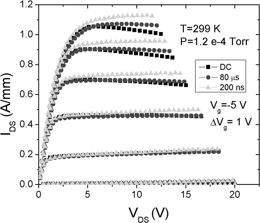
[0027] The same result is also observed for devices passivated by other dielectric layers, for example, devices pas...
PUM
 Abstract
Description
Claims
Application Information