A gallium nitride mis-hemt passivation design and preparation method thereof

A MIS-HEMT, gallium nitride technology, applied in the field of high electron mobility transistor HEMT, can solve the problems of high annealing temperature, increased on-resistance, current collapse, etc., achieves a simple preparation method, improves breakdown voltage, and leakage current. low effect

Active Publication Date: 2021-11-19
HUAZHONG UNIV OF SCI & TECH
View PDF4 Cites 0 Cited by
  • Summary
  • Abstract
  • Description
  • Claims
  • Application Information

AI Technical Summary

Problems solved by technology

[0004] 1. Conventional gallium nitride electronic devices are depletion-type, and the device will be turned on under zero bias, resulting in potential safety hazards in power electronics applications
[0005] 2. The ohmic contact of gallium nitride devices introduces gold, and the annealing temperature is very high, which is incompatible with the existing CMOS process
[0006] 3. When the GaN device is switched from the off state to the on state, the saturation current decreases and the on-resistance increases, that is, the current collapse phenomenon, which greatly affects the reliability of the GaN device application.
[0007] 4. At present, GaN devices have achieved gratifying results compared with silicon devices in terms of withstand voltage, but there is still a lot of room for improvement from its own theoretical value.

Method used


Image

  • A gallium nitride mis-hemt passivation design and preparation method thereof
  • A gallium nitride mis-hemt passivation design and preparation method thereof
  • A gallium nitride mis-hemt passivation design and preparation method thereof

Examples


Embodiment 1

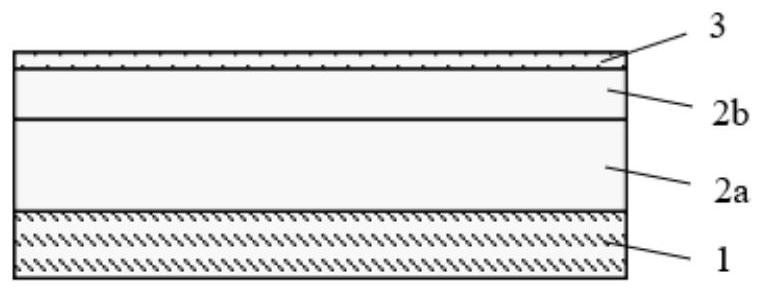
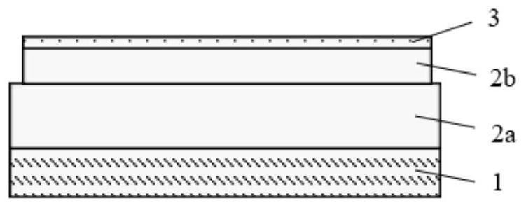
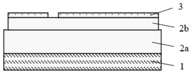
[0041] Generally speaking, the preparation of the present invention has a high dielectric constant dielectric gate dielectric, and the enhanced GaN power device after optimized passivation can be divided into 8 main steps, which are: processing the substrate, etching isolation, etching the gate Groove, sputtering ohmic metal, depositing gate dielectric, evaporating gate metal, sputtering P-type CuO passivation layer, depositing passivation layer.

[0042] This embodiment specifically includes the following steps:

[0043] Step 1, processing the substrate, figure 1 It is a sectional view of a silicon-based GaN substrate, and 1 in the figure is a Si (111) substrate. 2a in the figure is the epitaxial gallium nitride buffer layer. Because the substrate introduces Si and O atoms during the epitaxy process to form vacancies, that is, donor state defects in the buffer layer, electrons are released under the leakage voltage, resulting in large device leakage. At this time, acceptor ...


PUM

PropertyMeasurementUnit
breakdown field strengthaaaaaaaaaa

Abstract

The invention belongs to the technical field of semiconductor devices, and discloses a gallium nitride MIS-HEMT passivation design and a preparation method thereof, wherein the passivation structure includes twice stacked silicon-doped hafnium oxide HfSiO material and P-type CuO. Preferably, the MIS-HEMT device adopts a grooved gate structure; the gate dielectric adopts a high dielectric constant silicon-doped hafnium oxide material; the source and drain electrodes are prepared using a low-temperature gold-free contact process. The present invention improves the key composition and specific structure of the passivation structure, cooperates with the gate dielectric material of the GaN MIS-HEMT device, and utilizes two layers of high dielectric constant material (HfSiO) and low dielectric constant P-type oxide Comparing with the prior art, the present invention can realize better electrical performance by constructing the passivation structure by using CuO.

Description

technical field [0001] The invention belongs to the technical field of semiconductor devices, and more specifically, relates to a gallium nitride MIS-HEMT (ie, a high electron mobility transistor HEMT including a metal-insulator-semiconductor structure MIS; wherein, MIS means metal-insulator-semiconductor, HEMT stands for High Electron Mobility Transistor) passivation design and its preparation method, which can obtain gallium nitride MIS-HEMT devices with superior electrical properties. Background technique [0002] Since the advent of metal-oxide-semiconductor field-effect transistors, silicon materials have dominated the semiconductor industry. This is mainly due to the low cost of silicon semiconductors and the high-quality natural oxide layer on their surfaces. However, the narrow bandgap of silicon limits its development in the direction of power electronics, and it is inevitable to find semiconductor materials with better performance. Gallium nitride is a third-gener...

Claims


Application Information

Patent Timeline
Patent Type & Authority Patents(China)
IPC IPC(8): H01L29/778H01L29/06H01L21/335H01L29/423
CPCH01L29/0603H01L29/0684H01L29/42364H01L29/66431H01L29/778
Inventor 吴燕庆詹丹李学飞
Owner HUAZHONG UNIV OF SCI & TECH
Why Eureka
Try Eureka