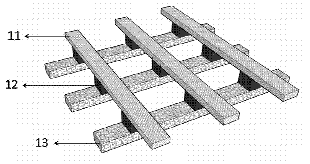
Resistive random access memory and manufacture method thereof
一种阻变存储、阻变的技术,应用在半导体器件、电固体器件、电气元件等方向,能够解决失去整流特性、驱动电流低、满足不了RRAM器件使用需求等问题,达到制作工艺容易、高集成度、降低Sneak电流的效果
- Summary
- Abstract
- Description
- Claims
- Application Information
AI Technical Summary
Problems solved by technology
Method used
Image

Examples
Embodiment Construction
[0024] The present invention will be further described below through specific embodiments and accompanying drawings.
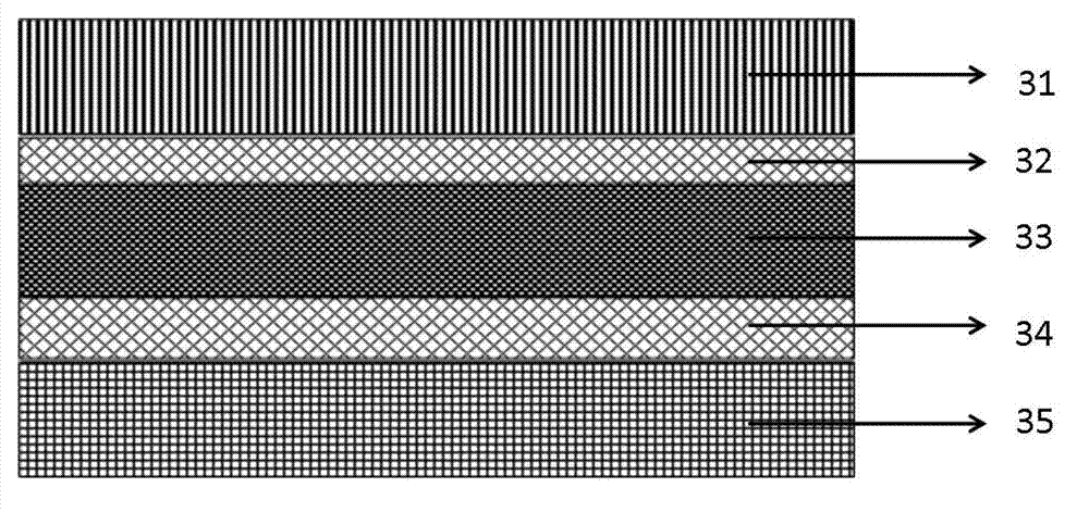
[0025] image 3 It is a schematic diagram of the structure of the RRAM storage unit of the resistive variable memory in this embodiment. The RRAM storage unit includes a metal upper electrode 31 ; a semiconductor metal oxide 32 ; a resistive switch material 33 ; a semiconductor metal oxide 34 ; and a metal lower electrode 35 . Since the semiconducting metal oxide is semiconducting, Schottky barriers are formed between the upper metal electrode 31 and the semiconducting metal oxide 32 and between the semiconducting metal oxide 34 and the lower metal electrode 35 . When the RRAM device is at low resistance, due to the existence of the Schottky barrier, the current flowing through the device at a lower voltage becomes smaller, thus effectively reducing the generation of Sneak current.
[0026] The preparation process of the above-mentioned RRAM storage unit will...
PUM
 Abstract
Description
Claims
Application Information
 - R&D
- Intellectual Property
- Life Sciences
- Materials
- Tech Scout
- Unparalleled Data Quality
- Higher Quality Content
- 60% Fewer Hallucinations
Browse by: Latest US Patents, China's latest patents, Technical Efficacy Thesaurus, Application Domain, Technology Topic, Popular Technical Reports.
© 2025 PatSnap. All rights reserved.Legal|Privacy policy|Modern Slavery Act Transparency Statement|Sitemap|About US| Contact US: help@patsnap.com