Balance microstrip line transition full-mode dual-ridged integrated waveguide feed dipole printed antenna
A technology of balancing microstrip lines and symmetrical oscillators, applied in the directions of antennas, electrical components, and radiating element structures, etc., can solve the problems of narrow single-mode operating bandwidth of substrate integrated waveguides and large radiation loss of antennas, and achieve compact structure and size. Small and miniaturized
- Summary
- Abstract
- Description
- Claims
- Application Information
AI Technical Summary
Problems solved by technology
Method used
Image
Examples
specific Embodiment approach 1
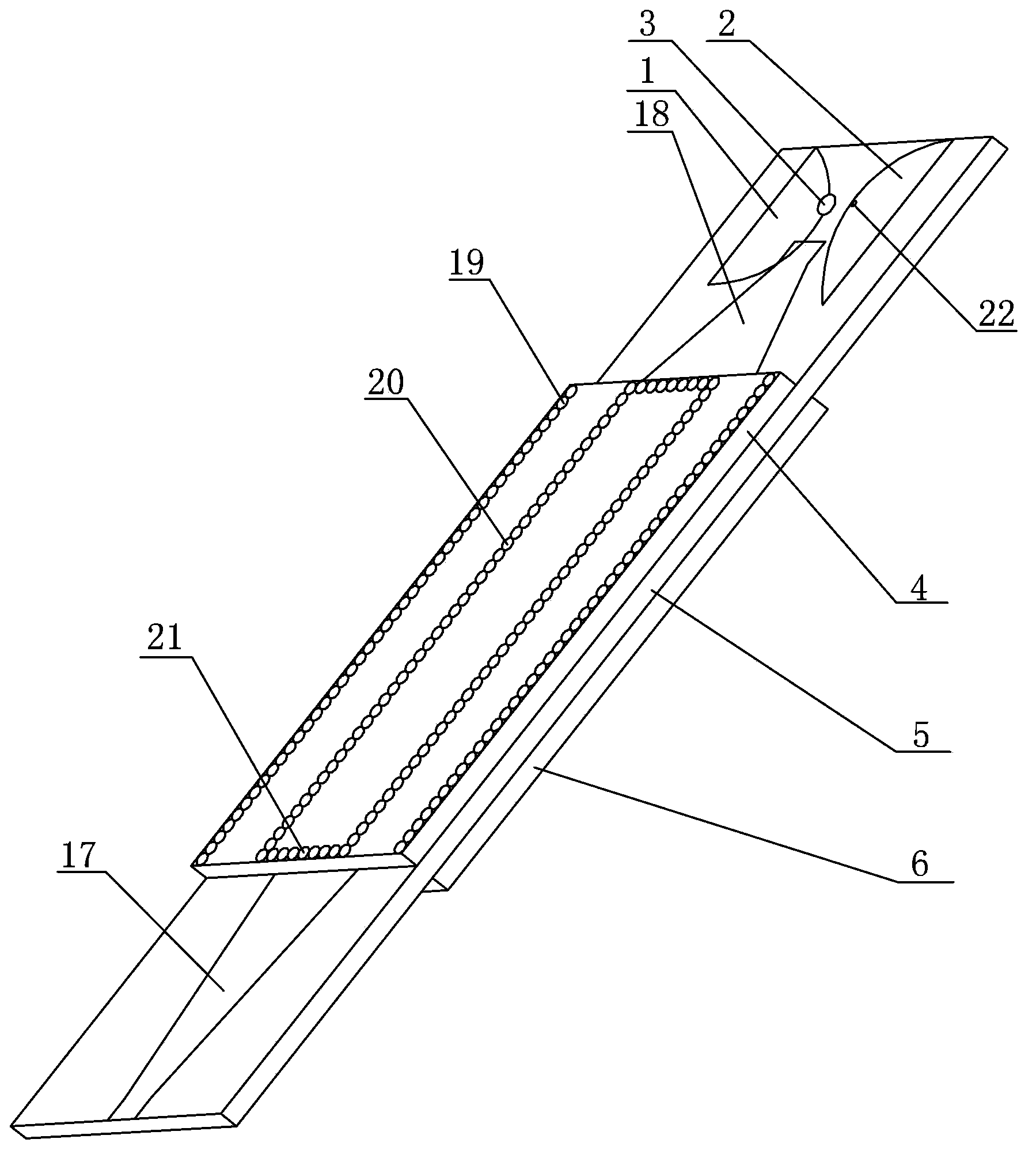
[0010] Specific implementation mode one: combine Figure 1 to Figure 10Describe this embodiment. The balanced microstrip line transition full-mode double-ridge integrated waveguide-fed symmetrical oscillator printed antenna in this embodiment includes a semicircular symmetrical oscillator assembly, a loading disc 3, an upper dielectric substrate 4, and a middle dielectric substrate. 5. The lower dielectric substrate 6, the metal patch on the upper dielectric substrate 7, the metal patch on the upper dielectric substrate 8, the metal patch on the lower dielectric substrate 9, the metal patch 10 on the lower dielectric substrate, and the upper dielectric substrate Metal patch 11, metal patch 12 under the middle dielectric substrate, metal transition piece 23, metal strips 13 under the two upper dielectric substrates, metal strips 14 on the two middle dielectric substrates, two lower dielectric substrates Metal strip 15, two metal strips 16 on the lower dielectric substrate, two ...
specific Embodiment approach 2
[0013] Specific implementation mode two: combination Figure 5 to Figure 10 Describe this embodiment, the length of the upper dielectric substrate 4 of the balanced microstrip line transition full-mode double-ridge integrated waveguide-fed symmetrical oscillator printed antenna described in this embodiment is 50 mm, the width of the upper dielectric substrate 4 is 35 mm, and the upper dielectric substrate 4 is 35 mm wide. The thickness of the substrate 4 is 1.5mm, the length of the middle dielectric substrate 5 is 112mm, the width of the middle dielectric substrate 5 is 35mm, the thickness of the middle dielectric substrate 5 is 1.5mm, and the length of the lower dielectric substrate 6 is 50mm, The width of the lower dielectric substrate 6 is 35mm, the thickness of the lower dielectric substrate 6 is 1.5mm, the length of the metal patch 11 on the middle dielectric substrate is 50mm, and the width of the metal patch 11 on the middle dielectric substrate is 16mm. The thickness o...
specific Embodiment approach 3
[0014] Specific implementation mode three: combination Figure 7 and Figure 8 Describe this embodiment. The balanced microstrip line transition full-mode double-ridge integrated waveguide integrated waveguide-fed symmetrical oscillator printed antenna in this embodiment has a radius of 11 mm, a radius of the right oscillator 2 is 11 mm, and a wafer 3 is loaded. The radius is 2 mm, and the distance L1 between the left vibrator 1 and the right vibrator 2 is 2 mm. Other components and connections are the same as those in the first embodiment.
PUM
 Abstract
Description
Claims
Application Information


