Delay control circuit applied to memory unit and static random access memory

A technology of delay control and level control, applied in the field of circuits, can solve the problems of large area, high cost, complex circuit, etc., and achieve the effect of reducing discharge speed, small leakage current and realizing delay.

Inactive Publication Date: 2013-02-06
SUZHOU UNIV
View PDF3 Cites 5 Cited by
  • Summary
  • Abstract
  • Description
  • Claims
  • Application Information

AI Technical Summary

Problems solved by technology

[0005] In view of this, the present invention provides a delay control circuit applied to memory cells to overcome the problems of complex circuits, large areas and high costs caused by the use of dual-column dummy cells in the prior art

Method used


Image

  • Delay control circuit applied to memory unit and static random access memory
  • Delay control circuit applied to memory unit and static random access memory
  • Delay control circuit applied to memory unit and static random access memory

Examples


Embodiment

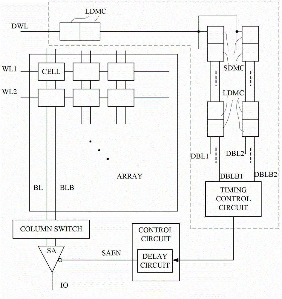
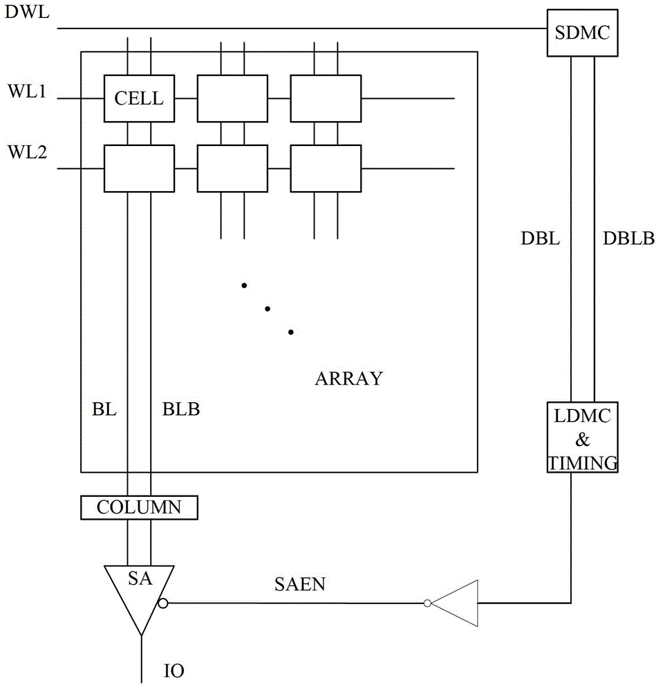
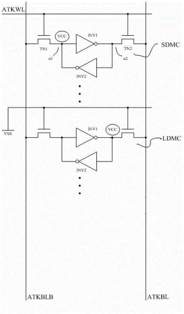
[0037] see Figure 4 , provides a circuit diagram of a delay control circuit applied to memory cells for the present invention, including: a control voltage divider circuit 101, a selection circuit 102, and a pull-down circuit 103, and the pull-down circuit includes a first NMOS transistor N0 and a second NMOS transistor pipe N1;

[0038] Wherein, the control voltage divider circuit 101 compares the virtual word line signal and the external control signal, and outputs the first control signal and the first control level VTHA, and the selection circuit 102 is used to receive the first control signal, and according to the The first control signal outputs a second control level VTHB, wherein the first control level VTHA controls the turn-on and turn-off of the second NMOS transistor, and the second control level VTHB controls the first NMOS transistor When the voltage Vcc is greater than the first preset value, the first NMOS transistor and the second NMOS transistor work in the...


PUM


Abstract

The invention provides a delay control circuit applied to a memory unit. The delay control circuit applied to the memory unit comprises a control voltage-dividing circuit, a selecting circuit and a pull-down circuit, wherein voltage VCC is larger than a first preset value, a first NMOS (N-channel metal oxide semiconductor) tube and a second NMOS tube in the pull-down circuit work in a saturated region; and when the voltage VCC is smaller than the second preset value, the second NMOS tube works in a sub-threshold region. The delay control circuit provided by the invention can ensure that the second NMOS tube works in the sub-threshold region in case of a relatively low working voltage, has very small leakage current and can lower the discharge rate of a dummy bit line (DBL), so that the delay of a sense amplifier control signal SAEN can be achieved; when the SAEN signal reaches, a read-out BL and a read-out BLB of a memory array have a relatively large differential pressure dELTaV which is easily read out by the amplifier; and circuit functions are ensured to be correct and have no logic error.

Description

technical field [0001] The invention relates to the field of circuits, more specifically, to a delay control circuit applied to a storage unit and a static random access memory. Background technique [0002] With the continuous development of technology, SRAM is widely used due to the characteristic that its cells can save data without refreshing. Usually, for a normal SRAM, the working voltage is generally kept above 0.9Vcc, which can ensure good storage performance. However, due to the problem of low process technology or actual working voltage, logic errors and functional failures in specific read operations of the SRAM are caused. At the same time, the reduction of the operating voltage will inevitably lead to the reduction of the operating speed. [0003] see figure 1 , the existing technology usually adopts a method of changing the control signal of the sense amplifier to solve the above-mentioned problem, specifically, a dual column dummy cell is used to generate t...

Claims


Application Information

Patent Timeline
Patent Type & Authority Applications(China)
IPC IPC(8): G11C11/413
Inventor 张立军郑坚斌王子欧张其笑季爱明毛凌峰朱灿焰
Owner SUZHOU UNIV
Why Eureka
Try Eureka