Thin film field effect transistor array substrate, manufacture method and display device thereof

A transistor array and thin film field effect technology, which is applied in semiconductor/solid-state device manufacturing, optics, instruments, etc., can solve problems such as pixel charging difficulties, and achieve the effects of reducing area, reducing lateral electric field, and reducing overlapping area

Inactive Publication Date: 2013-02-13
BOE TECH GRP CO LTD +1
View PDF8 Cites 8 Cited by
  • Summary
  • Abstract
  • Description
  • Claims
  • Application Information

AI Technical Summary

Problems solved by technology

Due to the characteristics of the ADS mode liquid crystal display, in this pixel electrode structure, the overlapping area between the pixel electrode and the common electrode is relatively large, resulting in the C between the pixel electrode and the common electrode. st (storage capacitance) is relatively large, making it difficult to charge the pixel

Method used


Image

  • Thin film field effect transistor array substrate, manufacture method and display device thereof
  • Thin film field effect transistor array substrate, manufacture method and display device thereof
  • Thin film field effect transistor array substrate, manufacture method and display device thereof

Examples


Embodiment 1

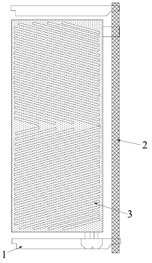
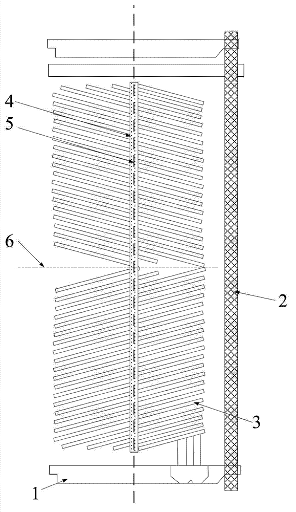
[0034] figure 2 Shown is a schematic structural view of the pixel electrode of the thin film field effect transistor array substrate of this embodiment, as figure 2 As shown, the thin film field effect transistor array substrate of this embodiment includes a plurality of gate lines and data lines, the gate lines and data lines are arranged perpendicular to each other; the sub-pixel area defined by the crossing of the gate lines and data lines; and A plurality of strip-shaped pixel electrodes formed in the sub-pixel area, wherein the thin film field effect transistor array substrate further includes: each strip-shaped pixel electrode arranged in the middle of each sub-pixel area, parallel to the data line 2 and connected to the sub-pixel area 3 are connected to a pixel electrode connection line 4.

[0035] Wherein, the sub-pixel area has a center line 5 parallel to the data line 2 (ie, the first center line) and a center line 6 parallel to the gate line 1 (ie, the second cen...

Embodiment 2

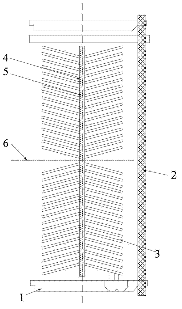
[0039] image 3 Shown is a schematic structural view of the pixel electrode of the thin film field effect transistor array substrate of this embodiment, as image 3 As shown, the thin film field effect transistor array substrate of this embodiment includes a plurality of gate lines and data lines, the gate lines and data lines are arranged perpendicular to each other; the sub-pixel area defined by the crossing of the gate lines and data lines; and A plurality of strip-shaped pixel electrodes formed in the sub-pixel area, wherein the thin film field effect transistor array substrate further includes: each strip-shaped pixel electrode arranged in the middle of each sub-pixel area, parallel to the data line 2 and connected to the sub-pixel area 3 are connected to a pixel electrode connection line 4.

[0040] Among them, the sub-pixel area has a center line 5 parallel to the data line 2 (ie, the first center line) and a center line 6 parallel to the gate line 1 (ie, the second cent...


PUM


Abstract

The invention provides a thin film field effect transistor array substrate, a manufacture method and a display device thereof and belongs to the field of liquid crystal display. The thin film field effect transistor array substrate comprises a plurality of grid lines, a plurality of data lines, sub pixel regions, a plurality of strip-shaped pixel electrodes formed in each sub pixel region and pixel electrode connection wires, wherein the grid lines are perpendicular to the data lines, the sub pixel regions are defined by crossing the grid lines and the data lines, and the pixel electrode connection wire is parallel to the data line and is connected with all the strip-shaped pixel electrodes in each sub pixel region. According to the technical scheme, display effects can be optimized.

Description

technical field [0001] The invention relates to the field of liquid crystal display, in particular to a thin film field effect transistor array substrate, a manufacturing method thereof, and a display device. Background technique [0002] TFT-LCD (Thin Film Transistor-Liquid Crystal Display, Thin Film Field Effect Transistor-Liquid Crystal Display) panel is generally composed of a TFT array substrate that acts as a switch and a color filter substrate coated with RGB, and then fills the liquid crystal between the two substrates Floor. Wherein, the TFT array substrate forms a gate layer, a source and drain layer, a pixel electrode and a common electrode layer after deposition and etching of various layers of films. [0003] In the Advanced Super Dimension Switch (ADS) liquid crystal display mode, the traditional pixel electrode structure such as figure 1 As shown, a plurality of strip-shaped pixel electrodes 3 are formed in the sub-pixel area. The strip-shaped pixel electrod...

Claims


Application Information

Patent Timeline
Patent Type & Authority Applications(China)
IPC IPC(8): G02F1/1362G02F1/1368G02F1/1343H01L21/77
Inventor 高玉杰
Owner BOE TECH GRP CO LTD
Why Eureka
Try Eureka