

Annealing method of sapphire substrate transfer graphene
A sapphire substrate and graphene technology, applied in the direction of gaseous chemical plating, coating, electrical components, etc., can solve problems such as poor contact and graphene influence, and achieve the effect of eliminating adverse effects
- Summary
- Abstract
- Description
- Claims
- Application Information
AI Technical Summary
Problems solved by technology
Method used
Image

Examples
Embodiment 1
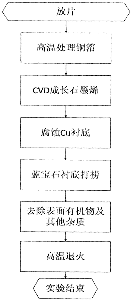
[0022] The realization steps of the present invention are as follows:
[0023] Step 1, high temperature treatment of copper foil.
[0024] Put the copper foil in the reaction chamber, pass H into the reaction chamber 2 , the copper foil was treated with a flow rate of 5 sccm, a temperature of 900° C., a time of 60 min, and an air pressure of 15 Torr.
[0025] Step 2, CVD growth of graphene.
[0026] Introduce Ar and CH to the reaction chamber 4 , keeping Ar and CH 4 The flow ratio is 10:1, Ar flow 200sccm, CH 4 The flow rate is 20 sccm, the air pressure is maintained at 1 Torr, the temperature is 900° C., and the heating and holding time are 20 minutes in total.
[0027] Step 3, etching the Cu substrate.
[0028] In Fe(NO 4 ) 3 Soak it in an aqueous solution (0.15g / ml) for 30 minutes, use the sapphire substrate to pick it up, and heat it in the air for 60 minutes, keeping the temperature at 150°C.
[0029] Step 4, removing surface organic matter.
[0030] Soak in ace...
Embodiment 2
[0037] The realization steps of the present invention are as follows:
[0038] Step A, high temperature treatment of copper foil.
[0039] Put the copper foil in the reaction chamber, pass H into the reaction chamber 2 , to treat the copper foil, the flow rate is 10sccm, the temperature is 950°C, the time is 40min, and the air pressure is 25Torr
[0040] Step B, CVD growth of graphene.
[0041] Introduce Ar and CH to the reaction chamber 4 , keeping Ar and CH 4 The flow ratio is 5:1, Ar flow rate is 100 sccm, CH 4 The flow rate is 20 sccm, the air pressure is maintained at 1 Torr, the temperature is 950° C., and the heating and holding time are 40 minutes in total.
[0042] Step C, etching the Cu substrate.
[0043] In Fe(NO 4 ) 3 Soak it in an aqueous solution (0.1g / ml) for 40 minutes, use the sapphire substrate to pick it up, and heat it in the air for 60 minutes, keeping the temperature at 200°C.
[0044] Step D, removing surface organic matter.
[0045] Soak in a...
Embodiment 3
[0052] The realization steps of the present invention are as follows:
[0053] Step 1, high temperature treatment of copper foil.
[0054] Put the copper foil in the reaction chamber, pass H into the reaction chamber 2 , to treat the copper foil, the flow rate is 20sccm, the temperature is 1000°C, the time is 20min, and the air pressure is 50Torr
[0055] Step 2, CVD growth of graphene.
[0056] Introduce Ar and CH to the reaction chamber 4 , keeping Ar and CH 4 The flow ratio is 3:1, Ar flow rate is 180 sccm, CH 4 The flow rate is 60 sccm, the air pressure is maintained at 1 Torr, the temperature is 1100°C, and the heating and holding time is 20 minutes.
[0057] Step 3, etching the Cu substrate.
[0058] In Fe(NO 4 ) 3 Soak it in an aqueous solution (0.15g / ml) for 30 minutes, use the sapphire substrate to pick it up, and heat it in the air for 60 minutes, keeping the temperature at 160°C.
[0059] Step 4, removing surface organic matter.
[0060] Soak in acetone for ...
PUM
 Abstract
Description
Claims
Application Information