
Annealing method for transferring graphene from sapphire substrate

A sapphire substrate and graphene technology, applied in the direction of gaseous chemical plating, coating, electrical components, etc., can solve problems such as poor contact and graphene influence, and achieve the effect of eliminating adverse effects and repairing graphene defects

Inactive Publication Date: 2015-07-29
XIDIAN UNIV
View PDF3 Cites 0 Cited by
  • Summary
  • Abstract
  • Description
  • Claims
  • Application Information

AI Technical Summary

Problems solved by technology

[0004] However, the graphene defects transferred to ordinary substrates using conventional transfer methods have many poor contacts, and it is difficult to effectively affect graphene. Therefore, it is urgent to invent a suitable post-transfer treatment method.

Method used


Image

  • Annealing method for transferring graphene from sapphire substrate

Examples


Embodiment 1

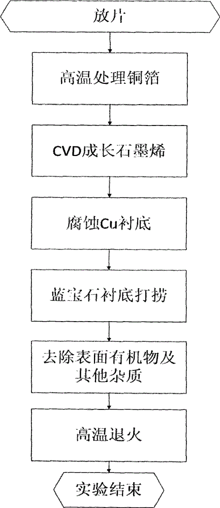
[0022] The realization steps of the present invention are as follows:

[0023] Step 1, high temperature treatment of copper foil.

[0024] Put the copper foil in the reaction chamber, pass H into the reaction chamber 2 , the copper foil was treated with a flow rate of 5 sccm, a temperature of 900° C., a time of 60 min, and an air pressure of 15 Torr.

[0025] Step 2, CVD growth of graphene.

[0026] Introduce Ar and CH to the reaction chamber 4 , keeping Ar and CH 4 The flow ratio is 10:1, Ar flow 200sccm, CH 4 The flow rate is 20 sccm, the air pressure is maintained at 1 Torr, the temperature is 900° C., and the heating and holding time are 20 minutes in total.

[0027] Step 3, etching the Cu substrate.

[0028] In Fe(NO 4 ) 3 Soak it in an aqueous solution (0.15g / ml) for 30 minutes, use the sapphire substrate to pick it up, and heat it in the air for 60 minutes, keeping the temperature at 150°C.

[0029] Step 4, removing surface organic matter.

[0030] Soak in ace...

Embodiment 2

[0037] The realization steps of the present invention are as follows:

[0038] Step A, high temperature treatment of copper foil.

[0039] Put the copper foil in the reaction chamber, pass H into the reaction chamber 2 , to treat the copper foil, the flow rate is 10sccm, the temperature is 950°C, the time is 40min, and the air pressure is 25Torr

[0040] Step B, CVD growth of graphene.

[0041] Introduce Ar and CH to the reaction chamber 4 , keeping Ar and CH 4 The flow ratio is 5:1, Ar flow rate is 100 sccm, CH 4 The flow rate is 20 sccm, the air pressure is maintained at 1 Torr, the temperature is 950° C., and the heating and holding time are 40 minutes in total.

[0042] Step C, etching the Cu substrate.

[0043] In Fe(NO 4 ) 3 Soak it in an aqueous solution (0.1g / ml) for 40 minutes, use the sapphire substrate to pick it up, and heat it in the air for 60 minutes, keeping the temperature at 200°C.

[0044] Step D, removing surface organic matter.

[0045] Soak in a...

Embodiment 3

[0052] The realization steps of the present invention are as follows:

[0053] Step 1, high temperature treatment of copper foil.

[0054] Put the copper foil in the reaction chamber, pass H into the reaction chamber 2 , to treat the copper foil, the flow rate is 20sccm, the temperature is 1000°C, the time is 20min, and the air pressure is 50Torr

[0055] Step 2, CVD growth of graphene.

[0056] Introduce Ar and CH to the reaction chamber 4 , keeping Ar and CH 4 The flow ratio is 3:1, Ar flow rate is 180 sccm, CH 4 The flow rate is 60 sccm, the air pressure is maintained at 1 Torr, the temperature is 1100°C, and the heating and holding time is 20 minutes.

[0057] Step 3, etching the Cu substrate.

[0058] In Fe(NO 4 ) 3 Soak it in an aqueous solution (0.15g / ml) for 30 minutes, use the sapphire substrate to pick it up, and heat it in the air for 60 minutes, keeping the temperature at 160°C.

[0059] Step 4, removing surface organic matter.

[0060] Soak in acetone for ...


PUM


Abstract

The invention discloses an annealing method of sapphire substrate transfer graphene. By adopting a high-temperature annealing mode, graphene defect generated in a substrate transfer process is repaired, and impurities which can not be removed in a transfer process or are newly introduced are further removed. Meanwhile, the high-temperature annealing can ensure that the contact of the substrate and the graphene is improved, influence of a sapphire substrate to the graphene is effectively processed, electric properties of the graphene attached on the sapphire substrate are optimized, and finally, the surface of the transferred graphene is cleaner, the defects are less, and the flat graphene is in better contact with the SiC substrate.

Description

technical field [0001] The invention belongs to the technical field of semiconductors, and relates to an annealing method for transferring graphene to a semiconductor substrate, in particular to an annealing method based on a sapphire (Al2O3) substrate, which can change the properties of the graphene material through the annealing after transferring to the substrate. Background technique [0002] As an emerging two-dimensional material, graphene has attracted widespread interest since its appearance. Among many peculiar properties, the mobility of graphene can reach 200,000cm-2v-ls-1 at room temperature. The reason why graphene Such a high mobility is caused by its unique energy band structure-theoretically, the effective mass of graphene carriers is zero. It is precisely because graphene has such excellent electrical properties that it is considered to have great potential for making high-speed and high-frequency devices. [0003] At present, there are three main methods f...

Claims


Application Information

Patent Timeline
Patent Type & Authority Patents(China)
IPC IPC(8): H01L21/324C23C16/56C23C16/26
Inventor 宁静王东韩砀闫景东柴正张进成郝跃
Owner XIDIAN UNIV
Learn More