Blue and green diode epitaxial slice and manufacturing method thereof

A technology of epitaxial wafers and diodes, which is applied in the field of diodes, can solve problems affecting the luminous efficiency of blue-green light-emitting diodes, and achieve the effect of improving luminous efficiency

Active Publication Date: 2013-02-13
HC SEMITEK ZHEJIANG CO LTD
View PDF3 Cites 7 Cited by
  • Summary
  • Abstract
  • Description
  • Claims
  • Application Information

AI Technical Summary

Problems solved by technology

Since the quantum barrier layer in contact with the P-type electron blocking layer in the MQW layer uses GaN as the growth material, and the P-type electron blocking layer covering it uses AlGaN as the growth material, so many electrons are blocked in the P-type electron blocking layer. In the quantum barrier layer in contact with the electron blocking layer, many holes also stay in this layer, and then many electrons and holes recombine in this layer, emitting light with a wavelength close to the ultraviolet band, which will affect the improvement of the luminous efficiency of blue-green LEDs

Method used


Image

  • Blue and green diode epitaxial slice and manufacturing method thereof
  • Blue and green diode epitaxial slice and manufacturing method thereof
  • Blue and green diode epitaxial slice and manufacturing method thereof

Examples


Embodiment 1

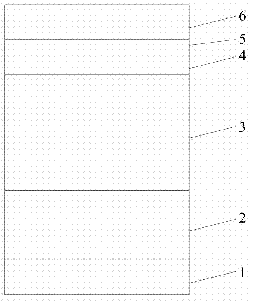
[0027] see figure 1 Embodiment 1 of the present invention provides a blue-green light diode epitaxial wafer, the epitaxial wafer includes a substrate layer 1, and a buffer layer 2, an N-type layer 3, a multi-quantum well layer 4, a P Type electron blocking layer 5 and P type layer 6.

[0028] Wherein, the substrate layer 1 includes but not limited to a sapphire substrate layer.

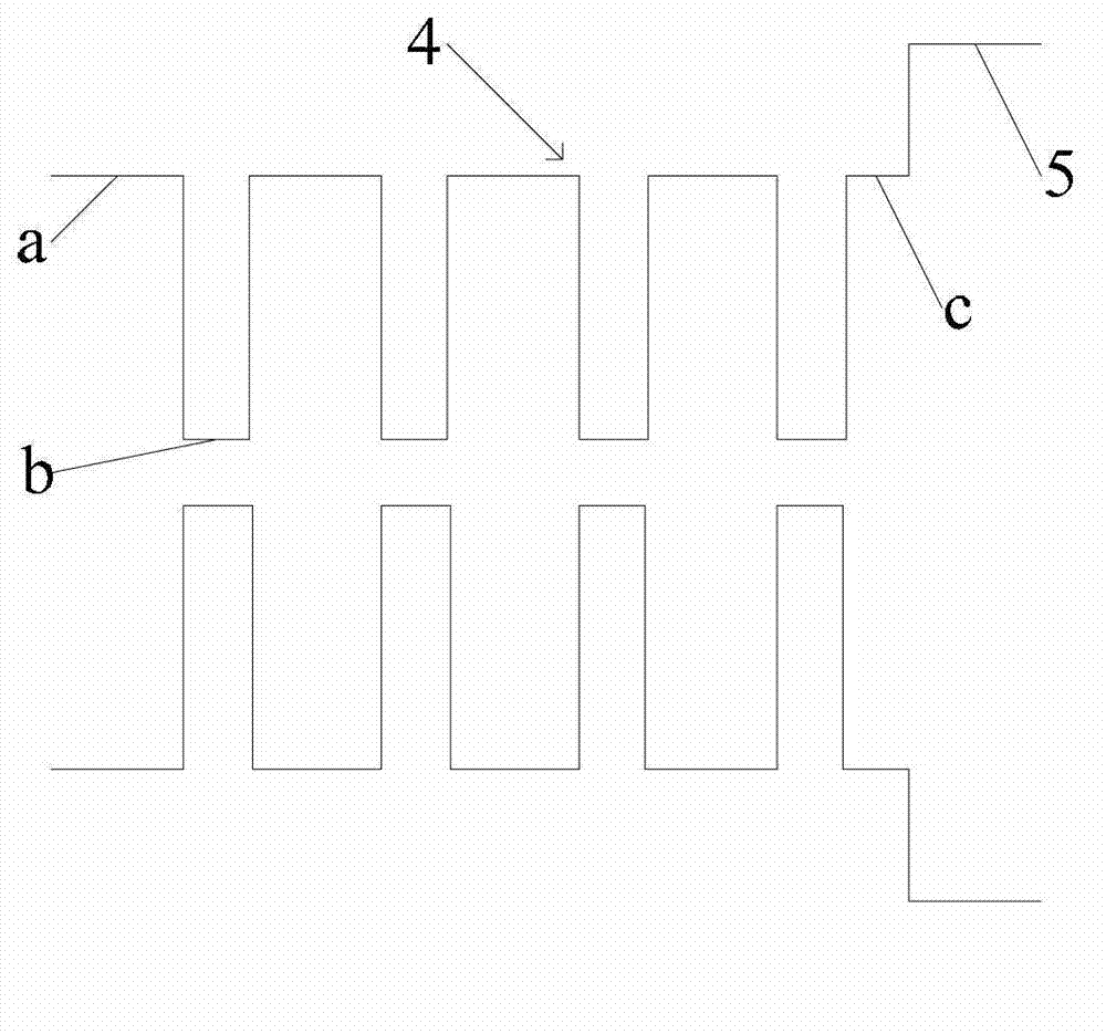
[0029] which, combined with figure 2 , the multi-quantum well layer 4 includes a composite layer formed alternately by several quantum barrier layers a and several quantum well layers b, and a transition layer c covering the composite layer. The layer in contact with the transition layer c in the composite layer is the quantum well layer b. The quantum barrier layer a uses GaN as a growth material, and the quantum well layer b uses InGaN as a growth material. The transition layer c also uses GaN as the growth material, but the thickness of the transition layer c is smaller than that of the quantu...

Embodiment 2

[0035] Embodiment 2 of the present invention provides a method for manufacturing a blue-green light diode epitaxial wafer, which is suitable for the blue-green light diode epitaxial wafer provided in Embodiment 1. The method includes:

[0036] 201 : growing a buffer layer 2 on the substrate layer 1 .

[0037] Specifically, the growth of the buffer layer 2 includes growth of a low-temperature buffer layer and growth of a high-temperature buffer layer. First, at a temperature of 625° C., a layer of non-doped GaN with a thickness of 30 nm is grown on the substrate layer 1 , which is a low-temperature buffer layer. Then, the temperature is raised to 1220° C., and a layer of non-doped GaN with a thickness of 3 μm is grown on the low-temperature buffer layer, which is a high-temperature buffer layer. So far, the growth of the buffer layer 2 is completed.

[0038] It is easy to know that before this step, the method further includes: cleaning the surface of the substrate layer 1 . ...

Embodiment 3

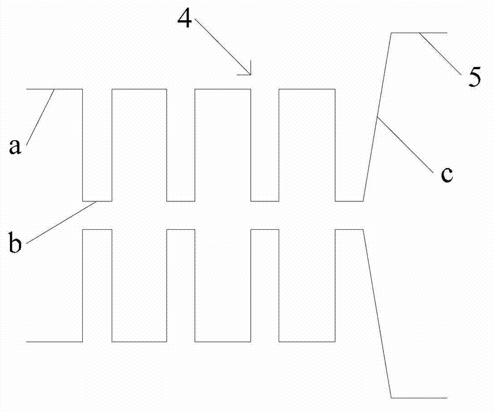
[0056] Embodiment 3 of the present invention provides a blue-green light diode epitaxial wafer. The structure of the epitaxial wafer is basically the same as that of the epitaxial wafer in Embodiment 1. The difference lies in that the combination image 3 , the composition of the transition layer c gradually changes from the growth material of the quantum well layer b to the growth material of the P-type electron blocking layer 5 . That is to say, in the composition of the transition layer c, the proportion of the growth material of the quantum well layer b gradually decreases, and the proportion of the growth material of the P-type electron blocking layer 5 gradually increases, and the composition of the transition layer c changes from all to The growth material of the quantum well layer b gradually becomes all the growth material of the P-type electron blocking layer 5 .

[0057] image 3 The energy band diagram of the multi-quantum well layer 4 and the P-type electron bloc...


PUM

PropertyMeasurementUnit
thicknessaaaaaaaaaa

Abstract

The invention discloses a blue and green diode epitaxial slice and belongs to the technical field of diodes. The epitaxial slice comprises a substrate layer and a buffering layer, an N-type layer, a multi-quantum well layer, a P-type electronic barrier layer and a P-type layer which sequentially cover the substrate layer, wherein the multi-quantum well layer comprises a composite layer and a transitional layer covering the composite layer and the composite layer consists of a plurality of quantum barrier layers and a plurality of quantum well layers which are arranged alternately; and one layer (in contact with the transitional layer) in the composite layer is the quantum well layer. According to the blue and green diode epitaxial slice, the translational layer replaces a quantum barrier layer (in contact with the P-type electronic barrier layer) in the multi-quantum well layer of the conventional epitaxial slice, so that the number of electrons stopped in the layer is reduced, and the number of cavities in the layer is also reduced; therefore, the electrons and the cavities which are compounded in the layer are reduced, and light of which the wavelength is close to that of the ultrasonic band is reduced; and finally, the luminous efficiency of a blue and green diode is improved.

Description

technical field [0001] The invention relates to the technical field of diodes, in particular to a blue-green light diode epitaxial wafer and a manufacturing method thereof. Background technique [0002] LED (Light Emitting Diode, light-emitting diode) chip is a semiconductor wafer, which is the core component of LED. The LED chip includes a GaN-based epitaxial wafer, and electrodes fabricated on the epitaxial wafer. [0003] The existing epitaxial wafer includes a substrate layer, a buffer layer, an N-type layer, a multi-quantum well layer, a P-type electron blocking layer and a P-type layer covering the substrate layer in sequence. Wherein, the multi-quantum well layer is a composite layer formed alternately by several quantum well layers and several quantum barrier layers. The layer in contact with the P-type electron blocking layer in the recombination layer is a quantum barrier layer. Usually, GaN is used as the growth material for the quantum barrier layer, InGaN is ...

Claims


Application Information

Patent Timeline
Patent Type & Authority Applications(China)
IPC IPC(8): H01L33/06H01L33/32H01L33/12H01L33/14
Inventor 吴克敏魏世祯
Owner HC SEMITEK ZHEJIANG CO LTD
Why Eureka
Try Eureka