Manufacture method of trench MOS (Metal Oxide Semiconductor) transistor
A technology of MOS transistor and manufacturing method, applied in the field of semiconductor manufacturing process
- Summary
- Abstract
- Description
- Claims
- Application Information
AI Technical Summary
Problems solved by technology
Method used
Image

Examples
Embodiment Construction
[0020] In order to make the content of the present invention clearer and easier to understand, the content of the present invention will be described in detail below in conjunction with specific embodiments and accompanying drawings.
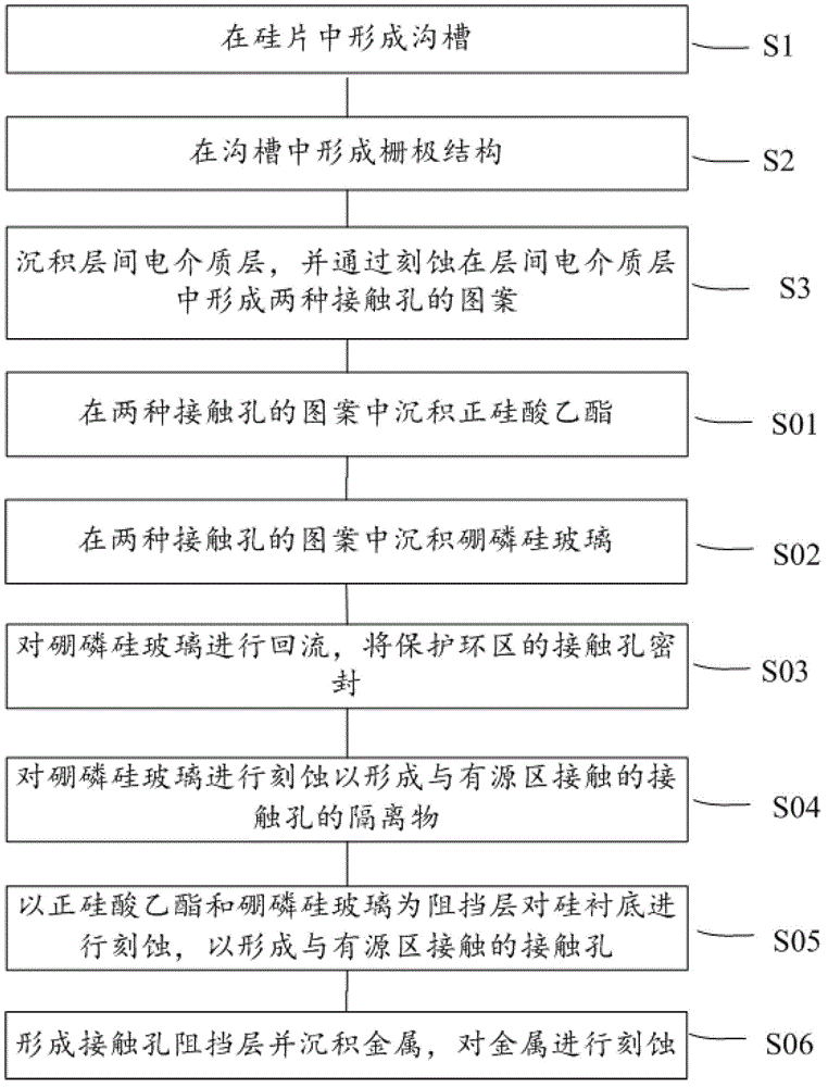
[0021] figure 2 A flow chart of a method for manufacturing a trench MOS transistor according to an embodiment of the present invention is schematically shown.
[0022] Such as figure 2 As shown, the method for manufacturing a trench MOS transistor according to an embodiment of the present invention includes:
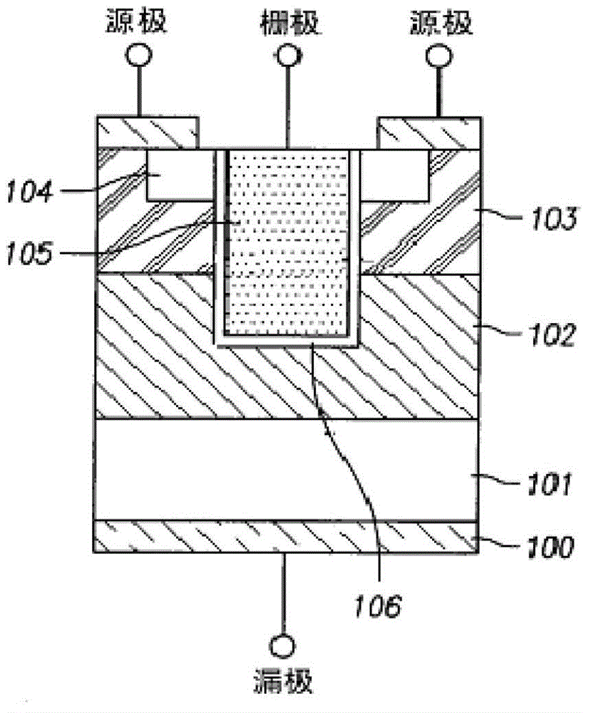
[0023] trench forming step S1, for forming trenches in the silicon wafer;
[0024] Gate structure forming step S2, for forming a gate structure in the trench;
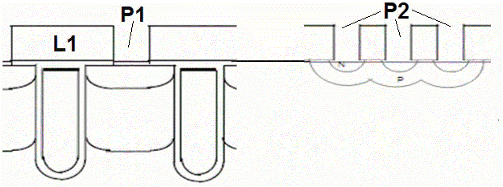
[0025] The interlayer dielectric deposition and etching step S3 is used to deposit the interlayer dielectric layer L1, and form two kinds of contact hole patterns in the interlayer dielectric layer by etching, one is corresponding to the contact hole contact with the active re...
PUM
 Abstract
Description
Claims
Application Information
 - R&D
- Intellectual Property
- Life Sciences
- Materials
- Tech Scout
- Unparalleled Data Quality
- Higher Quality Content
- 60% Fewer Hallucinations
Browse by: Latest US Patents, China's latest patents, Technical Efficacy Thesaurus, Application Domain, Technology Topic, Popular Technical Reports.
© 2025 PatSnap. All rights reserved.Legal|Privacy policy|Modern Slavery Act Transparency Statement|Sitemap|About US| Contact US: help@patsnap.com