High-voltage interconnection structure with practically-screened field plate
A technology of interconnection structure and field plate, applied in semiconductor/solid-state device components, electrical components, electric solid-state devices, etc.
- Summary
- Abstract
- Description
- Claims
- Application Information
AI Technical Summary
Problems solved by technology
Method used
Image

Examples
Embodiment Construction
[0024] In order to make the technical problems, technical solutions and beneficial effects to be solved by the present invention clearer, the present invention will be further described in detail below with reference to the accompanying drawings and embodiments. It should be understood that the specific embodiments described herein are only used to explain the present invention, but not to limit the present invention.
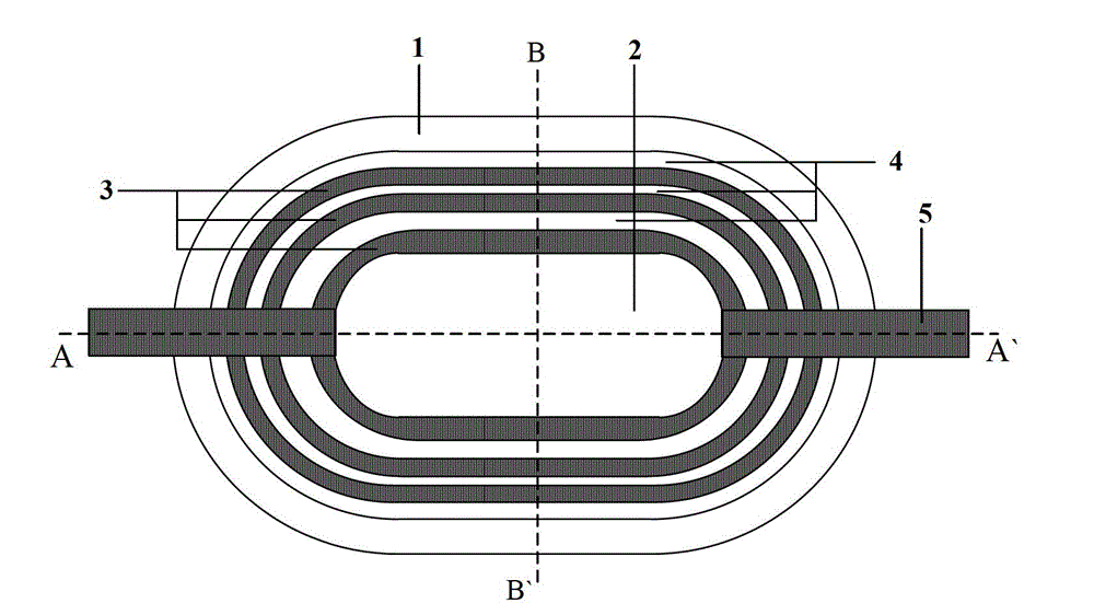
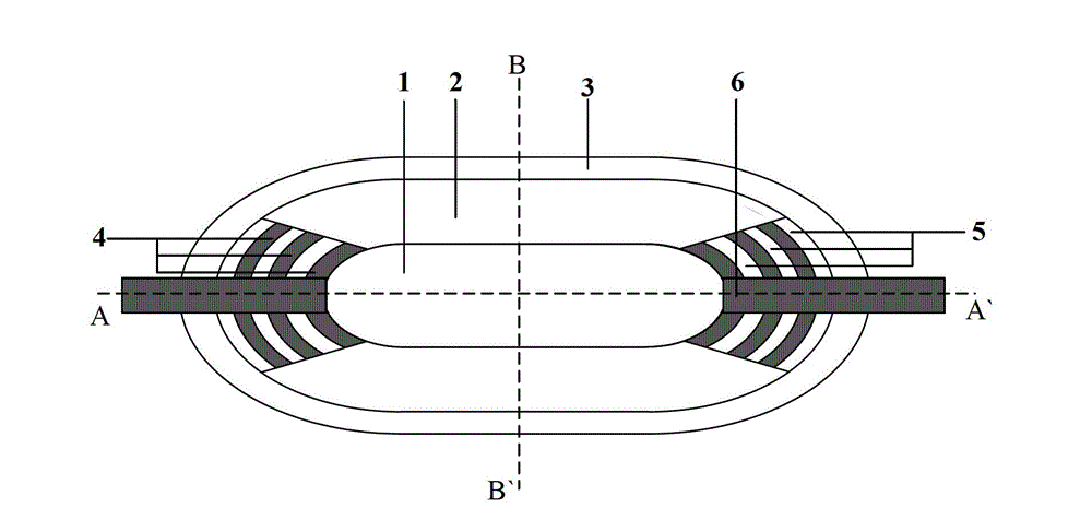
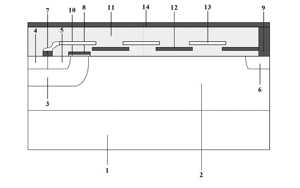
[0025] A high-voltage interconnect structure with partial field plate shielding for use in a racetrack-type lateral power device with high-voltage interconnect lines, comprising double-layer partial polysilicon shielding field plates and high-voltage interconnect lines; the double-layer partial polysilicon shielding The field plate exists only in the surface layer of the device crossed by the high-voltage interconnection line, and the surface of the device without the high-voltage interconnection line has no polysilicon shielding field plate; The second layer o...
PUM
 Abstract
Description
Claims
Application Information
 - R&D
- Intellectual Property
- Life Sciences
- Materials
- Tech Scout
- Unparalleled Data Quality
- Higher Quality Content
- 60% Fewer Hallucinations
Browse by: Latest US Patents, China's latest patents, Technical Efficacy Thesaurus, Application Domain, Technology Topic, Popular Technical Reports.
© 2025 PatSnap. All rights reserved.Legal|Privacy policy|Modern Slavery Act Transparency Statement|Sitemap|About US| Contact US: help@patsnap.com