Light-emitting diode of photonic crystal structure and application thereof

A technology of light-emitting diodes and photonic crystals, applied in semiconductor devices, electrical components, circuits, etc., can solve the problems of GaN-based LED compound luminous efficiency and low light extraction efficiency, and achieve the effect of improving light extraction efficiency and reducing ohmic contact resistance

Active Publication Date: 2014-12-17
SOUTHEAST UNIV
View PDF4 Cites 9 Cited by
  • Summary
  • Abstract
  • Description
  • Claims
  • Application Information

AI Technical Summary

Problems solved by technology

[0012] Technical problem: In view of the problems and deficiencies in the above-mentioned existing GaN-based LEDs with photonic crystal structures and their preparation methods, a light-emitting diode with a photonic crystal structure provided by the present invention can not only solve the problem of existing GaN-based LEDs The problem of low composite luminous efficiency and light extraction efficiency of LED can avoid the damage caused by the introduction of photonic crystals to the p-type GaN layer and the active region of the LED.

Method used


Image

  • Light-emitting diode of photonic crystal structure and application thereof
  • Light-emitting diode of photonic crystal structure and application thereof
  • Light-emitting diode of photonic crystal structure and application thereof

Examples


Embodiment Construction

[0028] The present invention will be further described below in conjunction with the accompanying drawings.

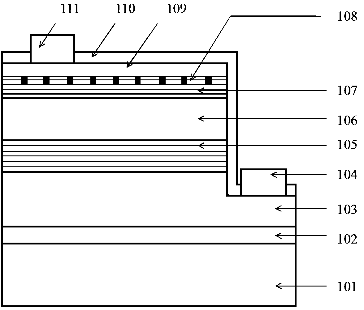
[0029] like figure 1 Shown is a side view of an LED with a novel photonic crystal structure provided by the present invention. The structural elements of the LED include: substrate 101, buffer layer 102, n-type GaN epitaxial layer 103, n-type electrode 104, active light-emitting layer 105 of InGaN / GaN multiple quantum wells, p-type GaN epitaxial layer 106, p-type super A lattice structure 107 , a photonic crystal structure 108 prepared in the p-type superlattice structure 107 , a transparent conductive layer 109 , a passivation layer 110 , and a p-type electrode 111 .

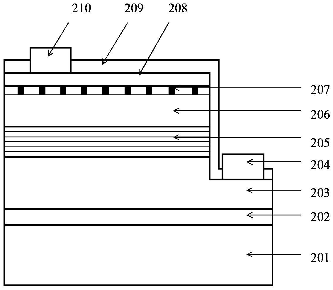
[0030] like figure 2 Shown is a side view of a prior art fabricated LED with a photonic crystal structure. Its constituent elements include: substrate 201, buffer layer 202, n-type GaN epitaxial layer 203, n-electrode 204, active light-emitting layer 205 of InGaN / GaN multiple quantum wells, p-type G...


PUM


Abstract

The invention provides a light-emitting diode of a photonic crystal structure. The light-emitting diode is provided with a substrate (101), a buffer layer (102), an n-type GaN epitaxial layer (103), an active luminescent layer (105) with InGaN / GaN multiple quantum wells, a p-type GaN epitaxial layer (106), a p-type super-lattice structure (107), a transparent conducting layer (109) and a passivation layer (110) in sequence from bottom to top, wherein an n-type electrode (104) is further arranged on the n-type GaN epitaxial layer (103); a p-type electrode (111) is further arranged on the transparent conducting layer (109); and a photonic crystal structure (108) is prepared in the p-type super-lattice structure (107). The light-emitting diode is applicable to a GaN-based LED (Light-emitting Diode), and is also applicable to other photo-electronic apparatuses which need to improve reflectivity of a certain wave band.

Description

technical field [0001] The invention belongs to the technical field of semiconductor optoelectronic device manufacturing, and mainly relates to a photonic crystal structure fabricated in a superlattice of an LED, which effectively reduces the p-type ohmic contact and improves the Manufacturing technology for LED light extraction efficiency. Background technique [0002] LED is currently the most widely used active device in the electronic information industry, and the high-brightness LED only releases a small amount of heat during the energy conversion process, which has the advantages of high efficiency, energy saving, environmental protection and long life, making it widely used in the fields of dynamic display and semiconductor lighting. It has a good application prospect. [0003] With the improvement of epitaxial growth technology, the brightness and efficiency of GaN-based LEDs have been significantly improved. However, in order to realize high-performance LED device...

Claims


Application Information

Patent Timeline
Patent Type & Authority Patents(China)
IPC IPC(8): H01L33/04H01L33/20H01L33/00
Inventor 张雄王春霞陈洪钧崔一平
Owner SOUTHEAST UNIV
Why Eureka
Try Eureka