

Acoustic wave element
An elastic wave and component technology, applied in electrical components, impedance networks, etc., can solve problems such as increased insertion loss and poor conductivity.
- Summary
- Abstract
- Description
- Claims
- Application Information
AI Technical Summary
Problems solved by technology
Method used
Image

Examples
Embodiment approach 1
[0066] Hereinafter, Embodiment 1 of the present invention will be described with reference to the drawings. figure 1 is a schematic cross-sectional view of the elastic wave device in Embodiment 1 (a schematic cross-sectional view perpendicular to the direction in which the IDT electrode fingers extend).
[0067] exist figure 1Among them, the elastic wave element 5 has: a piezoelectric body 6; an IDT electrode 7 provided on the piezoelectric body 6 and exciting a main elastic wave (Shear Horizontal wave, etc.) with a wavelength of λ; A silicon oxide film 8 covering the IDT electrode 7 and having a film thickness of not less than 0.20λ and less than 1λ. In addition, the wavelength λ of the main elastic wave is twice the electrode finger pitch. Furthermore, elastic wave element 5 includes dielectric thin film 9 provided on silicon oxide film 8 and propagating a transverse wave faster than the transverse wave propagating through silicon oxide film 8 . This elastic wave elemen...
Embodiment approach 2
[0104] Hereinafter, Embodiment 2 of the present invention will be described with reference to the drawings. Figure 8 It is a schematic cross-sectional view of an elastic wave device according to Embodiment 2 (a schematic cross-sectional view perpendicular to the direction in which the IDT electrode fingers extend). The same symbols are assigned to the same configurations as those in Embodiment 1, and description thereof will be omitted.
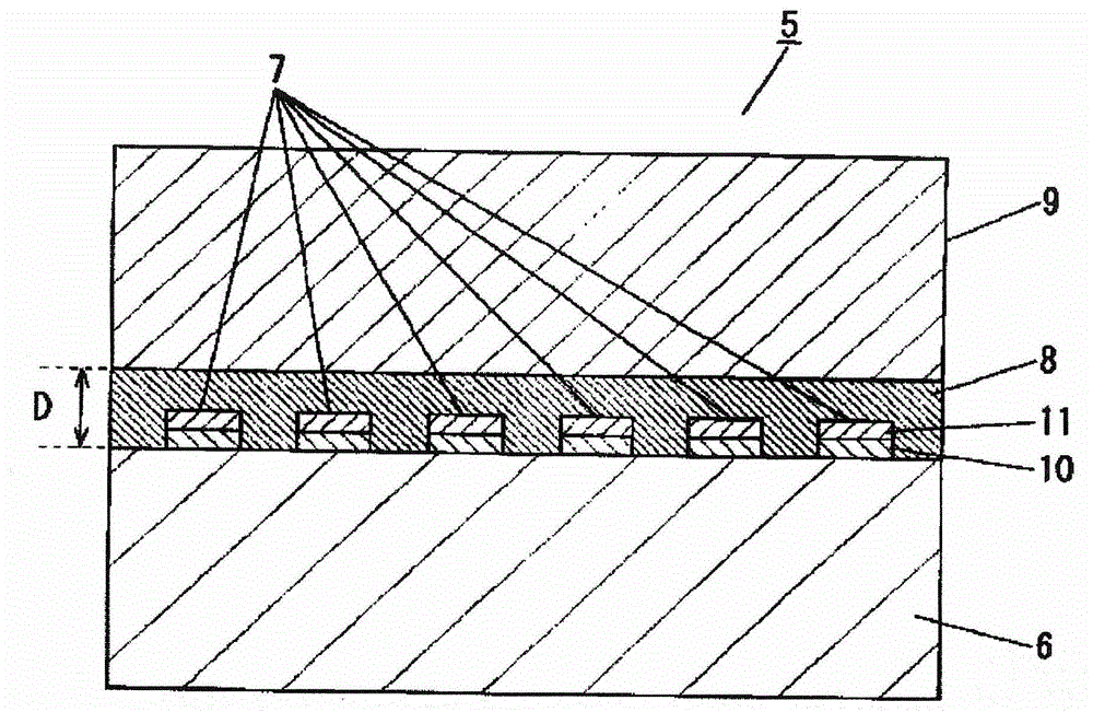
[0105] exist Figure 8 Among them, elastic wave element 5 does not include dielectric thin film 9 described in Embodiment 1, and is a surface wave element that distributes energy to the surface portion of piezoelectric body 6 or silicon oxide film 8 to excite main elastic waves.
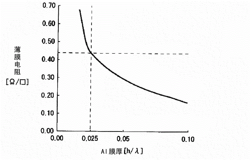
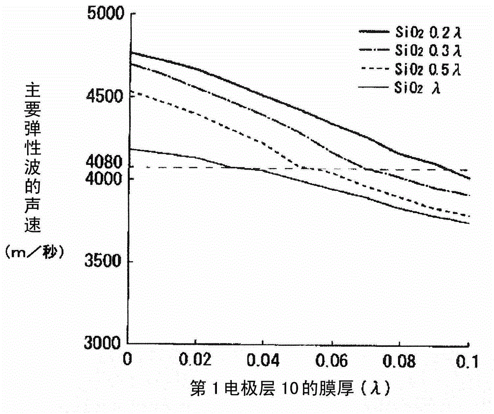
[0106] The IDT electrode 7 has a total film thickness of 0.15λ or less, the first electrode layer 10 has a film thickness of 0.03λ or more, and the second electrode layer 11 has a film thickness of 0.025λ or more.
[0107] The film thickness of the silicon oxide ...
Embodiment approach 3
[0146] Hereinafter, Embodiment 3 of the present invention will be described with reference to the drawings. Figure 15 is a schematic cross-sectional view of the elastic wave device in Embodiment 3 (a schematic cross-sectional view perpendicular to the direction in which the IDT electrode fingers extend).
[0147] In Embodiment 3, the main difference from Embodiment 1 is that the main component of the first electrode layer 10 is W (tungsten).
[0148] Figure 15 Among them, the elastic wave element 5 is provided with: a piezoelectric body 6; an IDT electrode 7 provided on the piezoelectric body 6 and exciting a main elastic wave (ShearHorizontal wave, etc.) with a wavelength of λ; The IDT electrode 7 and the silicon oxide film 8 having a film thickness of not less than 0.20λ and not more than 0.50λ. Furthermore, elastic wave element 5 includes dielectric thin film 9 that is provided on silicon oxide film 8 and that propagates a transverse wave faster than a transverse wave p...
PUM
 Abstract
Description
Claims
Application Information